| Objectives: To instill an understanding of how digital computers work from both a hardware and software perspective. |
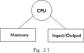
The Central Processing Unit (CPU) is the brain of the computer. It performs the essential task of fetching instructions from program memory and executing these instructions. The CPU contains the Arithmetic/Logic Unit (ALU) which performs the various arithmetic and boolean operations. The design of the ALU gives each computer its distinctive flavour. This is what makes the Intel 486 processor different from the Motorola 68000.
Memory is used for storage of program instructions as well as data. A unit of storage is called a word. Computers have different word lengths, for example, 4, 8, 12, 14, 16, 32 and 64-bit words are in common use today. Microcomputers generally use a word length of 8 bits, or a byte. Memory is organized as a linear array of words, a word being the smallest collection of bits which can be accessed by the CPU. Each word is identified by its address or location in memory. Thus a computer with 64K words of memory (65536) would require a memory address register that is 16 bits wide.
Semiconductor memories have virutally replaced older forms of memory such as magnetic core memory. Because of their highest density and lowest cost, dynamic random-access memory (DRAM) chips are used in modern computers. These have the drawback that they must be refreshed continuously. That is, additional control circuitry is required to access banks of memory periodically otherwise the electronic charge in each memory cell would be lost. DRAM are also volatile, i.e., all data is lost after the power is turned off. Static random-access memories (SRAM) are faster than DRAM, use less power and do not require refreshing. SRAM, like DRAM, are also volatile. There are may applications where non-volatile storage is required. Read-only memories (ROM) are used to store program code or information that never changes. To be cost effective, these must be programmed by the manufacturer in large quantities. UV-EPROM (ultra-violet erasable programmable ROM) can be erased and reprogrammed by the user using a special UV lamp and programming equipment. EEPROM (electrically erasable PROM) has the advantage of being erasable and programmable in situ. Flash memory is another form of EEPROM. Because of their higher density, block orientation and longer erase times, these are more suited as replacements for hard disk drives or as removable storage devices such as CompactFlash™ cards and memory sticks.
Without Input/Output (I/O) capabilities a computer would not be of much use. I/O is any means of getting information into and out of the computer. This could be as simple as switches and lights or more traditional I/O devices such as the keyboard, mouse and video display. Modems, sound cards, analog-to-digital and digital-to-analog converters, serial and parallel ports, timers and counters are all examples of I/O devices.
Storage devices fall into another category of I/O devices. Hard disk drives, floppy disk drives and CD-ROM drives are mass storage devices for keeping large amounts of information. While these may not be perceived as part of the I/O capabilities of the computer, from the hardware perspective they are interfaced to the computer via the I/O bus.
We are familiar with the computer in its most highly visible form as the personal computer (PC) and its aliases such as desk-top or lap-top computer, engineering work-station, business computer, file server and so on. Applications of the PC cover wide areas from personal, scientific, engineering, business and commercial applications to Internet servers, Information Management Systems (e.g. patient records, airline reservations) and industrial process controllers.
And yet there are more computers installed all over the world in areas other than the ones just described. These are the computers embedded in machines, instruments and appliances such as cameras, stereos, TVs, VCRs, microwave ovens, computer printers, copiers, modems, mobile phones, wristwatches, automobiles, test and diagnostic equipment, scientific equipment, health-care instruments and the list goes on and on.
Embedded computers refer to both microprocessors as well as more complex computer systems applied to a specific task. In most cases, the user is unaware of the computational engine under the cover and neither cares about the software or operating system being employed. Embedded processors range in size and cost from miniature 4-bit microprocessors costing under $1 to full blown Pentium or Power PC based systems costing in excess of $10,000.
(In July 2004 Freescale Semiconductor was created from the semiconductor division of Motorola.)
This course uses the Motorola 68HC11 as a model microcontroller unit (MCU) because its architecture and programmer's model is relatively simple. The fundamentals are universal and can be applied to any other microprocessor. Moreover, we will promote the idea that bigger does not mean better. Smallness can be beautiful. There are many obvious advantages to being small such as being compact, portable, energy efficient, simple to design and manufacture, less costly and more reliable.
The Motorola 68HC11 microprocessor is a low cost and yet very powerful 8-bit solution to many embedded processor applications. The HC11 is a large family of processors available from Motorola in various input/output configurations based on the same CPU core.
Here are some of the highlights of the MC68HC811
The earliest member of the family is the MC68HC11A1P which comes with 256 bytes SRAM and 512 bytes EEPROM in a 48-pin DIP package. The EEPROM space may be somewhat small for storing programs but is quite useful for saving non-volatile information such as setup, calibration or user defined settings.
 The processor you will be using in
the lab is the MC68HC811E2FN which comes with 256 bytes SRAM and 2K bytes of EEPROM in a 52-pin plastic
leaded chip carrier (PLCC) package. The advantage of having a relatively larger EEPROM is that we can store our
executable code in non-volatile memory directly via a serial link without having to worry about erasing a UV-EPROM
as with other processors/systems. With efficient assembly language coding it is amazing how much can be accomplished
in just 2K bytes of program memory.
The processor you will be using in
the lab is the MC68HC811E2FN which comes with 256 bytes SRAM and 2K bytes of EEPROM in a 52-pin plastic
leaded chip carrier (PLCC) package. The advantage of having a relatively larger EEPROM is that we can store our
executable code in non-volatile memory directly via a serial link without having to worry about erasing a UV-EPROM
as with other processors/systems. With efficient assembly language coding it is amazing how much can be accomplished
in just 2K bytes of program memory.
Figure 2.2 shows the register model of the ALU of the HC11 CPU.
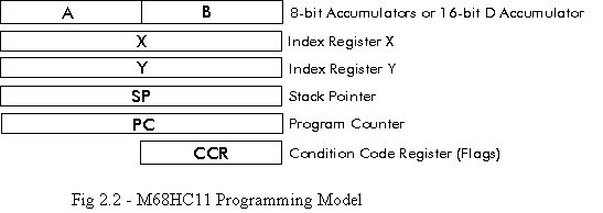
Accumulators A and B can be combined to form a single 16-bit accumulator (D). Thus, many 16-bit operations are available on this 8-bit microprocessor. The X and Y index registers are both 16-bit accumulators which are available for some 16-bit arithmetic. However, they are generally used to store 16-bit addresses in order to access data stored in memory. The program counter (PC) will contain the address of the next instruction to be executed. Similarly, the stack pointer (SP) contains the address of the next free space in SRAM which is available for temporary storage. (Stacks are explained in Chapter 4). In general, the programmer can consider the handling of the PC and SP as an internal matter and may ignore the two for the time being.
The Condition Code Register contains eight flags and control bits used to monitor the results of arithmetic/logic operations and to control certain CPU functions.
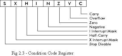
The Zero (Z) bit is set when the result of the last arithmetic, logical, or data manipulation is zero.
The Negative (N) bit reflects the state of the MSB of the result. For 2's complement notation, the N bit is set if the result is negative.
The Overflow (V) bit is used to indicate if an arithmetic overflow has occurred as a result of the operation.
The Carry (C) bit is used to indicate if a carry from an addition or a borrow from a subtraction has occurred. The C bit is also used in shift and rotate operations.
For the time being you may ignore the functions served by S, X, H and I bits.
A computer program is a set of precise instructions stored in memory for the CPU to act on. Instructions on the HC11 vary in length from 1 to 5 bytes, depending on the individual instruction. This is characteristic of a Complex Instruction Set Computer (CISC) as compared to a Reduced Instruction Set Computer (RISC). For example, the Pentium is a CISC while the Power PC is a RISC. How does the CPU of a CISC know how many bytes make up the instruction? The first byte in the sequence dictates the type of instruction and therefore the number of bytes to follow for that instruction. Therefore it makes no sense to execute program bytes out of synchronous order.
A machine cycle is defined as the shortest length of time it takes to perform an internal hardware operation. The HC11 used in the lab is driven by an 8MHz crystal oscillator. The machine clock frequency is ¼ of the oscillator frequency and therefore is 2MHz. Thus, a machine cycle is 500ns in duration. To fetch and execute an instruction may require a number of machine cycles.
A collection of instructions (i.e. the program) is stored in memory at sequential locations and the CPU fetches and executes each instruction one at a time. The flow of execution is controlled by the CPU with the use of the program counter. This register keeps track of the address of the next byte to be fetched.
Normally, the CPU will fetch instructions from memory in sequential order unless instructed to do otherwise as in the case of a jump or branch instruction. In this case, the PC will be loaded with a new memory address and on the next fetch cycle the flow of program execution will be directed to a different location in memory.
Pieces of data are stored in memory in exactly the same fashion as instructions. The CPU has no way of distinguishing instructions from data. Of course, the programmer knows which locations are used for data storage and will create the program such that data locations are never executed. In the event that this occurs, the program will behave unexpectedly and "crash".
What is the difference between machine language and assembly language? Machine language or machine code is the native language or instructions that the computer executes. Information on a digital computer is encoded using a two-state mechanism, that is, either ON or OFF. Therefore all information is manipulated and stored using a binary number system. Machine language is inherently a binary system.
Assembly language and machine language both represent the same information. They represent the native binary codes which will be entered into the computer and constitute a coherent set of instructions which we call the program. The difference lies in the interpretation by humans.
Machine code is binary. Programming a computer using the binary system of notation is very time consuming, inefficient and prone to errors. By utilizing decimal, octal and hexadecimal notation, it is possible to reduce the amount of data entry and book-keeping and therefore reduce effort and likelihood of errors. For example, the machine code to stop the CPU is 11001111. It is easier to write this as $CF, and even better to write STOP. Using hexadecimal formats or meaningful words is simply a better way for humans to relate to the binary instruction.
Instead of using a numeric value, either written as binary or hexadecimal, to represent an instruction, it is easier to use an acronym or mnemonic. The use of a mnemonic which has a one-to-one equivalence to the machine code and its function is called assembly language programming. The computer does not understand assembly language. Assembly language is a mechanism to assist humans in creating and managing programs in machine code more effectively and efficiently. Thus, programmers write in assembly language. Computers execute machine code.
When a program is written in assembly language, it must be translated into machine code and into a form that can be entered into the memory of the computer. This process is called assembling and can be accomplished manually. However, this is prone to errors and an automated method is preferred. A computer program which translates assembly language programs into machine code is called an assembler.
Simulators and debuggers are other program development tools which assist programmers in testing and debugging assembly language programs.
Assembly language programming is best introduced through the use of simple examples. Let us suppose we wish to find the sum of 12 and 23. In standard algebra we could write:
RESULT = 12 + 23
In HC11 assembly language, we have to instruct the CPU at each step of the operation. Here is a program to do this:
| LDA | #12 | |||
| LDB | #23 | |||
| ABA | ||||
| STA | RESULT | |||
| STOP |
Here is a brief explanation of the mnemonics and what each line does.
The machine codes for this program in hexadecimal notation are as follows:
86 0C C6 17 1B 97 00 CF
This program is of little use since we know the answer to be 35, a priori. Instead, it would be more useful to add two numbers whose values may be not fixed, i.e., what we call variables. Let us rephrase our example as:
RESULT = NUM1 + NUM2
The assembly language program to accomplish this may look as follows:
| LDA | NUM1 | |||
| LDB | NUM2 | |||
| ABA | ||||
| STA | RESULT | |||
| STOP |
The difference between the two examples above is the use of the immediate symbol (#) in the first two lines. In the first example, the # specifies that the numeric data is a constant value and this value is found in the byte or pair of bytes following the instruction op-code byte. This is called immediate addressing mode. In the second example, the omission of the # specifies that the symbols NUM1 and NUM2 represent addresses and the numeric data are stored at these memory addresses.
Thus, note the difference between the following two instructions:
| LDA | #4 | |||
| LDA | 4 |
| Misuse of the # symbol is a common source of programming error which the assembler cannot discern. |
| LDA | 4 | |||
| LDB | 5 |
In general, it is best not to use absolute addresses of variables. Instead, let the assembler assign memory addresses to symbols as it sees fit. Let us examine the memory model (or map) of the HC11.
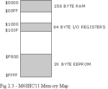
The memory map shows that the 256 bytes of SRAM reside from address $0000 to $00FF. This block of read/write memory will be used to store our variables as well as the stack. Our program code will be stored in 2K bytes of EEPROM starting at address $F800. The Input/Output features of the HC11 are accessible as a 64-byte block of memory with addresses from $1000 to $103F.
Here is the complete program to add two numbers with some assembler directives or pseudo-operations added.
| ORG | $0000 | |||
| NUM1 | DS | 1 | ||
| NUM2 | DS | 1 | ||
| RESULT | DS | 1 | ||
| ORG | $F800 | |||
| LDA | NUM1 | |||
| LDB | NUM2 | |||
| ABA | ||||
| STA | RESULT | |||
| STOP | ||||
| ORG | $FFFE | |||
| FDB | $F800 | |||
| END |
The statements in the gray area are the same CPU instructions as before. The statements added are not CPU instructions. These are called assembler directives or pseudo-ops and are used to direct the assembler during the assembly task. The first ORG statement sets the assembler's memory address to zero. This step is not necessary since the address is initialized to zero by default. The next three statements use the DS directive (Define Storage) to reserve space in SRAM for our three variables, NUM1, NUM2 and RESULT. Each of the three statements has two purposes. The first purpose is to define the memory address of the symbol or label shown to the left of the DS. The second purpose is to specify the number of bytes to reserve for that variable. In this example, NUM1, NUM2 and RESULT will be assigned the addresses 0, 1 and 2 respectively, each occupying one byte.
The second ORG directive in the program resets the assembler's memory address to $F800 which is the start of the EEPROM block where our machine code will be stored. This directive tells the assembler that the first byte of our program will begin at address $F800.
The third ORG directive resets the memory address to $FFFE. This points to the last two bytes of the EEPROM which will contain the reset vector, i.e. the starting address of the program. In these two bytes we store the 16-bit address $F800, which is the address of the first instruction.
Please refer to the description of assembler directives for more information.
Ignoring the assembler directives for the time being, here is another way to add our two numbers:
| LDA | NUM1 | |||
| ADDA | NUM2 | |||
| STA | RESULT | |||
| STOP |
The complete HC11 instruction set is listed here to familiarize you with the HC11 capabilities. For more information, see the HC11 Instruction Table. There are six addressing modes which refer to the different ways parameters are accessed. These modes are as follows:
In the inherent addressing mode, all of the information is contained in the instruction byte. The operands (if
any) are registers and no memory reference is required. These are one or two byte instructions. Here is a list
of all the inherent instructions:
| Mathematical Operations | ||
| ABA | Add B to A | |
| ABX | Add B to X | |
| ABY | Add B to Y | |
| CBA | Compare A to B | |
| CLRA | Clear A | |
| CLRB | Clear B | |
| COMA | 1's Complement A | |
| COMB | 1's Complement B | |
| DAA | Decimal Adjust A | |
| DECA | Decrement A | |
| DECB | Decrement B | |
| DES | Decrement Stack Pointer (S) | |
| DEX | Decrement X | |
| DEY | Decrement Y | |
| INCA | Increment A | |
| INCB | Increment B | |
| INS | Increment S | |
| INX | Increment X | |
| INY | Increment Y | |
| NEGA | 2's Complement A | |
| NEGB | 2's Complement B | |
| SBA | Subtract B from A | |
| TSTA | Test A | |
| TSTB | Test B | |
| Shift Operations | ||
| ASLA | Arithmetic Shift Left A | |
| ASLB | Arithmetic Shift Left B | |
| ASLD | Arithmetic Shift Left D | |
| ASRA | Arithmetic Shift Right A | |
| ASRB | Arithmetic Shift Right B | |
| LSLA | Logical Shift Left A (same as ASLA) | |
| LSLB | Logical Shift Left B (same as ASLB) | |
| LSLD | Logical Shift Left D (same as ASLD) | |
| LSRA | Logical Shift Right A | |
| LSRB | Logical Shift Right B | |
| LSRD | Logical Shift Right D | |
| ROLA | Rotate Left A | |
| ROLB | Rotate Left B | |
| RORA | Rotate Right A | |
| RORB | Rotate Right B | |
| Inter-Register Operations | ||
| TAB | Transfer A to B | |
| TBA | Transfer B to A | |
| TAP | Transfer A to Condition Code Register | |
| TPA | Transfer Condition Code Register to A | |
| TSX | Transfer Stack Pointer to X | |
| TSY | Transfer Stack Pointer to Y | |
| TXS | Transfer X to Stack Pointer | |
| TYS | Transfer Y to Stack Pointer | |
| XGDX | Exchange D with X | |
| XGDY | Exchange D with Y | |
| PSHA | Push A onto Stack | |
| PSHB | Push B onto Stack | |
| PSHX | Push X onto Stack | |
| PSHY | Push Y onto Stack | |
| PULA | Pull A from Stack | |
| PULB | Pull B from Stack | |
| PULX | Pull X from Stack | |
| PULY | Pull Y from Stack | |
| Flag Operations | ||
| CLC | Clear Carry | |
| CLI | Clear Interrupt Mask | |
| CLV | Clear Overflow Flag | |
| SEC | Set Carry | |
| SEI | Set Interrupt Mask | |
| SEV | Set Overflow Flag | |
| Miscellaneous Operations | ||
| IDIV | Integer Divide D ÷ X => X, remainder in D | |
| FDIV | Fractional Divide D ÷ X, for D < X, => X ÷ 216 , remainder in D | |
| MUL | Multiply A × B => D | |
| NOP | No Operation | |
| RTI | Return from Interrupt | |
| RTS | Return from Subroutine | |
| STOP | Stop Microprocessor | |
| SWI | Software Interrupt | |
| WAI | Wait for Interrupt | |
The HC11 is capable of performing arithmetic and logical operations on memory locations as well as the A, B and D accumulators. Thus the programming model is not restricted to the A and B 8-bit accumulators. This makes implementation of multiple-precision arithmetic possible. For example, it is relatively easy to program the 8-bit HC11 to process 32-bit integers.
The size of the operand, i.e., one or two bytes, is determined by the size of the accumulator or register used. For example, the instruction STD to store the D accumulator requires a 2-byte destination and will write into two sequential memory locations. The first memory location receives the MSB (accumulator A) and the next location receives the LSB (accumulator B). That is, bytes are stored in the high-byte/low-byte order. This is the opposite to most Intel processors.
In the immediate addressing mode, the actual argument is contained in the one or two bytes immediately following the instruction byte, where the number of bytes must match the size of the register being used. Thus the actual constant value is stored as part of the sequence of bytes that make up the instruction. This mode is selected when the # symbol precedes the argument. Examples:
| LDA | #23 | |||
| SUBD | #ONE | |||
| ANDA | #$F0 |
In the direct addressing mode (also called page zero addressing) a single byte is used to specify the least significant byte of the 16-bit memory address of the parameter to be accessed. The MSB of this effective address is assumed to be $00. Therefore only addresses $0000 to $00FF are accessible using direct addressing. Instructions using direct addressing are two byte instructions and therefore make more efficient use of machine cycles and memory space. Examples:
| STA | 1 | |||
| STD | RESULT | |||
| LSR | NUM |
In the extended addressing mode, two bytes are required to specify the full 16-bit effective address of the parameter to be referenced. Hence the full range of address from $0000 to $FFFF can be specified. Examples:
| LDA | table | |||
| STB | PORTA | |||
| JSR | output |
In indexed addressing mode, one of the index registers (X or Y) is used in calculating the effective address. The effective address is the contents of the specified indexed register (X or Y) plus the 8-bit unsigned value following the opcode byte. This mode of addressing is useful for accessing individual items or elements of an array or for sequencing through the array. Examples:
| LDA | PORTB,X | |||
| DEC | 3, Y | |||
| BSET | PORTA X $F0 |
The HC11 does not have an indirect addressing mode. This information is included to round out the discussion on memory addressing modes. Indirect addressing is one of the most powerful and sometimes confusing features available on most computers and yet the concept is fairly simple. With direct (as well as extended) addressing the effective address is specified in the instruction bytes. In indirect addressing mode, the memory location specified by the instruction bytes contains the effective address of the parameter.
In many programming operations, we are not so much concerned about the actual contents of a variable but more about the location of the variable. That is, many times our focus is on the address of a variable and how to manipulate this address. In high level languages such as Pascal and C, structures and pointers rely heavily on the use of indirect addressing. On the HC11, indexed addressing mode is used to implement indirect addressing.
| Memory-Accumulator Operations | ||
| ADCA | Add with Carry A | |
| ADCB | Add with Carry B | |
| ADDA | Add Memory to A | |
| ADDB | Add Memory to B | |
| ADDD | Add 16-bit to D | |
| ANDA | AND A with Memory | |
| ANDB | AND B with Memory | |
| BITA | Bit Test A with Memory | |
| BITB | Bit Test B with Memory | |
| CMPA | Compare A to Memory | |
| CMPB | Compare B to Memory | |
| CPD | Compare D to 16-bit (also CMPD) | |
| CPX | Compare X to 16-bit (also CMPX) | |
| CPY | Compare Y to 16-bit (also CMPY) | |
| EORA | Exclusive OR A with Memory | |
| EORB | Exclusive OR B with Memory | |
| LDAA | Load Accumulator A (also LDA) | |
| LDAB | Load Accumulator B (also LDB) | |
| LDD | Load Accumulator D with 16 bits | |
| LDS | Load Stack Pointer with 16 bits | |
| LDX | Load Index Register X with 16 bits | |
| LDY | Load Index Register Y with 16 bits | |
| ORAA | OR Accumulator A | |
| ORAB | OR Accumulator B | |
| SBCA | Subtract with Carry from A | |
| SBCB | Subtract with Carry from B | |
| STAA | Store Accumulator A (also STA) | |
| STAB | Store Accumulator B (also STB) | |
| STD | Store Accumulator D | |
| STS | Store Stack Pointer | |
| STX | Store Index Register X | |
| STY | Store Index Register Y | |
| SUBA | Subtract Memory from A | |
| SUBB | Subtract Memory from B | |
| SUBD | Subtract 16-bit from D | |
| Memory-Only Operations | ||
| ASL | Arithmetic Shift Left | |
| ASR | Arithmetic Shift Right | |
| CLR | Clear Memory | |
| COM | 1's Complement | |
| DEC | Decrement Memory | |
| INC | Increment Memory | |
| LSL | Logical Shift Left (same as ASL) | |
| LSR | Logical Shift Right | |
| NEG | 2's Complement | |
| ROL | Rotate Left | |
| ROR | Rotate Right | |
| TST | Test for zero or minus | |
The relative addressing mode is used only for branch instructions. If the branch condition is true, the 8-bit signed integer following the instruction opcode is added to the current contents of the program counter (PC) to form the effective branch address. If the branch is not taken, program execution continues with the next instruction. Examples
| BNE | main | |||
| BSR | putc | |||
| loop | BRCLR | FLAGS $80 loop |
| Branching - Unsigned Arithmetic | ||
| BHI | Branch if Higher | |
| BHS | Branch if Higher or Same (same as BCC) | |
| BLO | Branch if Lower (same as BCS) | |
| BLS | Branch if Lower or Same | |
| Branching - 2's Complement Signed Arithmetic | ||
| BGE | Branch if Greater than or Equal to zero | |
| BGT | Branch if Greater Than zero | |
| BLE | Branch if Less than or Equal to zero | |
| BLT | Branch if Less Than zero | |
| General Branching | ||
| BCC | Branch if Carry is Clear | |
| BCS | Branch if Carry is Set | |
| BEQ | Branch if EQual to zero | |
| BMI | Branch if MInus | |
| BNE | Branch if Not Equal to zero | |
| BPL | Branch if PLus | |
| BRA | BRanch Always | |
| BRN | BRanch Never | |
| BVC | Branch if oVerflow is Clear | |
| BVS | Branch if oVerflow is Set | |
| BSR | Branch to SubRoutine | |
| Long Branch | ||
| JMP | Jump to new location (16-bit address) | |
| JSR | Jump to SubRoutine (16-bit address) | |
| (Technically speaking, these are not relative branch instructions but are absolute jumps using extended addressing mode. These two instructions are listed here to complete the list of branch instructions.) | ||
Another powerful feature of the HC11 is the ability to set or clear any individual bit or pattern of bits of RAM or I/O register using the BSET and BCLR instructions. In either operation, the target address is specified followed by a bit mask. Only the bits of the target byte whose corresponding bits in the bit mask are 1's will be affected. All other bits in the target byte are unaffected. Note that these two instructions are restricted to direct addressing ($00 to $FF) and index addressing.
| Bit Set/Clear | ||
| BSET | Bit Set | |
| BCLR | Bit Clear | |
| Branching if Bit Set/Clear | ||
| BRSET | Branch if bits set | |
| BRCLR | Branch if bits clear | |
Examples:
| BSET | NUM, %01000001 | ;set bits 6 and 0 of NUM | |
| BCLR | PORTA, X $80 | ;clear bit 7 of PORTA | |
| BRSET | NUM $01 MAIN | ;branch if bit 0 of NUM is set | |
Programs are created using a text editor or any word processor which can produce a text file. The syntax and format for program statements must follow the following rules.
Any text following the semi-colon (;) is treaded as a comment. This style of comment may appear anywhere on the line. An asterix (*) placed at the leftmost position on the line also defines the line as a comment.
| ******************************************************************* | ||||
| * | These are comment lines | |||
| ******************************************************************* | ||||
| ; This also a comment | ||||
| LDA | NUM1 | ;this is a comment after an instruction | ||
Labels or symbols are used for user defined constants, variables, memory addresses and subroutine names. The actual value assigned to the label is expected to be an 8-bit or 16-bit value. The label name may contain upper and lower case letters as well as numerals but no punctuation marks. Label names are case sensitive, for example, PortA and portA are different symbols. Label names should not be more than 10 characters in length.
Labels or symbols are defined when they appear at the leftmost position on the line. The assembler assigns to the label a value that is equal to the current memory address. Labels must not be defined more than once otherwise the assembler will flag an M error, multiple definition attempted. The current memory addess is automatically updated as bytes are occupied, whether for program or data storage.
If the EQU directive is specified then the value appearing in the parameter field, instead of the current memory address, is assigned to the label. The current memory address remains unchanged.
Here are some examples of label definitions:
| EEPROM | EQU | $F800 | ||
| PORTB | EQU | $1004 | ||
| PA7 | EQU | %1000000 | ||
| ten | EQU | 10 | ||
| * When deciding which format to use, choose the one | ||||
| * that best describes the object | ||||
| num1 | DS | 2 | ||
| start | LDA | num1 | ||
| ADDA | #ten | |||
| What is the difference between the following statements: LDA #123 LDA #$7B LDA #%01111011 The answer is none. 123, $7B and %01111011 are just different notations or representations for us humans to represent the same quantity or value which is One Hundred and Twenty Three. The bit pattern stored on the computer is 01111011 and is always binary. |
The assembler can perform limited arithmetic in the expression field. Only a single operation is allowed per expression and the operator must be separated from the parameters by white space. The operators are
| + | add | |
| - | subtract | |
| * | multiply | |
| / | integer divide | |
| % | modulus |
The assembler performs this arithmetic at assembly time. That is, the result of the expression is resolved during assembly and becomes a constant value or memory address. One place where this can be useful is when accessing individual bytes of a multiple byte parameter. For example, suppose NUM is declared as a 4-byte number, then we can access each individual byte as NUM, NUM + 1, NUM + 2 and NUM + 3.
| NUM | DS | 4 | ;reserve 4 bytes for NUM | |
| LDA | NUM | ;fetches MSB | ||
| LDB | NUM + 3 | ;fetches LSB | ||
| * note that the assembler assumes that the first byte reserved is the MSB | ||||
| * followed by the less significant bytes | ||||
ORG - Set the assembler's memory address to a new origin.
The ORG directive sets the assembler's current memory address to the value specified in the operand field. If no ORG directive is specified, the memory address is initialized to $0000. Examples:
| ORG | $F800 | |||
| ORG | EEPROM |
END - End of assembly
The END directive indicates to the assembler the end of the program. Any statements following the END directive are treated as comments and are not assembled.
EQU - Equate symbol to a value
The EQU directive assigns the value of the expression in the operand field to the label. The EQU directive assigns a value other than the current memory address to the label. The label cannot be redefined anywhere else in the program. The expression must not contain any forward references or undefined symbols. Examples:
| EEPROM | EQU | $F800 | ||
| ten | EQU | 10 |
FCB - Form Constant Byte (also DB - Define Byte)
The FCB directive stores a byte into the current memory location. Examples:
| CR | FCB | $0D | ||
| ONE | FCB | 1 |
FCC - Form Constant Character
The FCC directive stores a single byte representing the ASCII code the specified character. Examples:
| charA | FCC | A | ||
| quote | FCC | " | ||
| ZERO | FCC | 0 |
Note the differences with the following statements:
| ZERO | EQU | 0 | ;nothing is stored in memory |
| ZERO | FCB | 0 | ;$00 is stored at current PC |
| ZERO | FCC | 0 | ;$30 is stored at current PC |
FCS - Form Constant String
The FCS directive places a sequence of bytes representing the ASCII codes of the characters in the specified string. The first non-space character following FCS is the string delimiter and is not part of the string. The string consists of all characters following the delimiter up to, and not including, the next delimiter. The sequence of bytes stored is terminated with a zero byte. Examples:
| mess | FCS | 'This is a string' |
| title | FCS | $This is another string |
| text | FCS | "The second delimiter is not needed |
FDB - Form Double Byte constant (also DW - Define Word)
The FDB directive places a double byte (16-bits) at the current memory location. The high order byte is placed in the lower of the the memory addresses. Examples:
| num | FDB | 1234 | ||
| vect | FDB | $FFFE | ||
| rstrt | FDB | start |
RMB - Reserve Memory Bytes (also DS - Define Storage)
The DS or RMB directive reserves the specified number of bytes at the current memory address. The memory address counter is then advanced by the specified number of bytes. Examples:
| num | DS | 1 | ;reserve 1 byte |
| result | DS | 4 | ;create a 32-bit result |
| buffer | DS | 16 | ;create a buffer of 16 bytes |
| A | Addressing error, relative address is out of range | |
| B | not a Binary character | |
| D | not a Decimal character | |
| H | not a Hexadecimal character | |
| I | Illegal instruction | |
| M | Multiple definition of label attempted | |
| P | Phase error, value of label differs in 1st and 2nd pass | |
| S | Syntax error | |
| U | Undefinded symbol | |
| X | Extended address error, address must be single byte |
Example 1 - Toggle output at PD5
In our first programming example to add two numbers the RESULT is stored in the computer's SRAM and there is no way of verifying the result. As stated before, any computation or computer program is of no use if the computer cannot communicate with the real world (is this an inverse oxymoron or what?). The simplest thing the program can do to indicate that it is running is for it to send out some pulses via an output pin which can be observed using an oscilloscope. Example 1 shows one simple way of getting the CPU to indicate such activity to the outside world. This is a useful feature and can be utilized in the future when debugging your programs.
Example 1 begins by declaring certain hardware constants such as the EEPROM address and the PORTD and DDRD addresses. Note that the full 16-bit extended addresses are used in this example. Only six bits of PORTD are available on the chip and these are labelled from PD0 to PD5. Each of the 6 lines to PORTD bits are bidirectional, that is, they can be configured to be input or output lines, independent of each other. In order to specify which lines are input or output, we use the Data Direction Register for PORTD, called by the label DDRD. A 1 set in a bit position of DDRD will set the corresponding bit of PORTD as an output line. The default setting of DDRD is all zeros, that is, all the PORTD bits are set as inputs. Note that this is the fail-safe mode.
PD5 is declared as an 8-bit mask where the position of the 1 in the bit pattern %00100000 specifies bit-5. Here it is more meaningful to use a binary specifier rather than decimal. A hexadecimal constant of $20 will work just as well.
The first instruction of the program begins at address $F800 which is labelled as start. Accumulator A is loaded with the bit pattern for PD5 and this value is written to DDRD in order to set the direction for output. The same pattern is written to PORTD in order to set PD5 to logic 1. The next instruction clears all of the bits of PORTD even though we are only concerned with PD5. The CPU branches back to the label called main in order to repeatedly send out a train of pulses on PD5. The CPU is therefore stuck in an infinite loop.
The next ORG changes the memory address to point to the last two bytes of EEPROM which is called the reset vector. In these two bytes we will store, using the FDB directive, the 16-bit address representing the start of our program. This happens to be $F800 which was the value assigned to the label start.
| This lengthy discussion of Example 1 and the examples to follow is for the student's benefit only. In general, you do not have to elaborate in this manner in your exercises. You make the assumption that a person reviewing your program has a basic knowledge of assembly language programming and the HC11 instruction set. Instead of explaining what each instruction does, you should outline what you are trying to accomplish in more general terms. |
Example 1a - Toggle output pin at PD5 using extended addressing mode
and BSET/BCLR.
In the previous Example 1, extended addresses are used to reference the I/O addresses. By doing so, all bits in PORTD and DDRD are accessed simultaneously. Sometimes it is desirable to access a single bit or group of bits independently from the other bits. This can be accomplished using the BSET and BCLR instructions. However, these instructions are available in the direct addressing and indexed addressing modes only. In direct addressing, the operand is an 8-bit page zero address. For indexed addressing mode, the operand is an 8-bit offset which is added to the contents of index register X or Y to form the effective address.
Example 1a also shows how the BSET and BCLR instructions are used to access PD5 output bit. Here we declare the I/O registers' base address to be $1000 and PORTD and DDRD are defined using their 8-bit offsets only, namely $08 and $09 respectively. The program begins by initializing the X index register to the base address and uses the BSET instruction to set the PD5 direction register for output. In the main program loop, we set and clear bit-5 of PORTD using the BSET and BCLR instructions using indexed addressing mode with register X as the index register.
This example shows how to display messages on the Liquid Crystal Display. This is a very important way of testing and debugging your programs and will be covered in more detail in Chapter 3.
Note that this example uses both extended and indexed addressing modes in order to access the I/O locations.
The HC11 prototyping board comes with an RS-232 serial port. This example shows how to use this communications port and is covered in Chapter 3.
The 68HC11 comes with a built-in 8-channel 8-bit analog to digital converter. This example shows how to initialize the ADC and how to take readings.
HC11 Reference Manual 332 pages, 3279KB pdf