Motorola created computer landmarks, namely, the 6800, 6809 and 68000 microcomputers. Offsprings of these CISC (complex instruction set computer) continue to add to the list of processors available while bringing more powerful features. The 6809, a landmark in its own right, never achieved the prominence that it deserved. However, it, along with the 6800, laid the foundation for future generations of 8-bit and 16-bit processors. These include the 6802, 6805, HC11, HC12 and HC16. The family heritage is seen in the CPU (central processing unit), instruction set and memory-mapped input/output schemes adopted by the various families of processors.
The Motorola MC68HC908 is an incremental improvement to the 6805 family of 8-bit MCU (microcontroller unit). This family is designed for simple, low cost, low computational power, low power consumption, embedded applications, in other words, simple controllers.
In keeping with the theme of simplicity, we will focus on one particular group of MCUs from the HC908 family - the HC908QT1, HC908QT2, HC908QT4, HC908QY1, HC908QY2 and HC908QY4.
|
QT1
|
QT2
|
QT4
|
QY1
|
QY2
|
QY4
|
|
| Package Size (pins) |
8
|
8
|
8
|
16
|
16
|
16
|
| Flash Memory Size (bytes) |
1536
|
1536
|
4096
|
1536
|
1536
|
4096
|
| ADC |
-
|
yes
|
yes
|
-
|
yes
|
yes
|
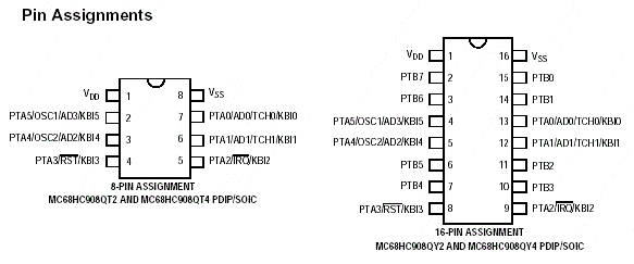
The differentiating features are shown in the Feature Table. Because there is very little difference in features and costs we will focus entirely on the MC68HC908QY4 available in a 16-pin package. For applications where no more than six input/output (I/O) are required, the HC908QT4, in an 8-pin package will most certainly be attractive. For the most compact solutions, choose the surface mount packages.
The ubiquitous 555 timer is a handy device for creating timer and oscillator circuits. You can easily cascade two or more 555 timers to create delay-timers, sequencers, PLCs or whatever you may want to call them. But before using the 555 timer in your next timer/sequencer project, consider using an HC908 instead.
|
LMC555 Timer
|
68HC908QT1
|
|
| Price US$ (as of Dec 2003) |
$0.54
|
$2.02
|
| Package |
8-pin DIP
|
8-pin DIP
|
| Supply Voltage |
2-15V
|
3-5V
|
| Supply Current |
100uA
|
5mA
|
| Minimum Delay |
1uS
|
1uS
|
| Maximum Delay |
1 hour?
|
infinite
|
| Trigger Inputs |
1
|
5 max
|
| Reset Inputs |
1
|
5 max
|
| Outputs |
1
|
5 max
|
| Inverted Outputs |
NO
|
YES
|
| Waveform Output |
Simple
|
Any
|
| External Components |
2R + 1C
|
None
|
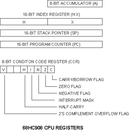
The diagram shows the programming model of the CPU of the 68HC908 MCU. The classic model of a single-accumulator CPU consists of a single 8-bit register called the accumulator (A). While this register is the primary holding place for manipulating all data, the 8-bit index register (X) can also assist in most numerical operations. The original design of the 6805 CPU core uses a single 8-bit index register. This made it difficult to work with arrays of data exceeding 256 memory locations. Motorola has recognized this deficiency and has added an H-register whose primary intent is to extend the index register to 16 bits. Thus indexed addressing operations can now cover the full 65536 range of memory addresses without too much fuss.
|
While the use of a single 8-bit accumulator may appear to be somewhat restrictive, Motorola's programming model for all of its CISC MCUs allows operations on SRAM locations and input/output (I/O) registers as if they were accumulators. This greatly simplifies programming tasks and makes multi-precision arithmetic (32-bit integers for example) relatively straight forward. |
The stack is an area of memory taken from SRAM that is used for storing subroutine return addresses, register data during interrupts, subroutine parameters and local variables. The Stack Pointer (SP) is a 16-bit register which points to the next available memory of the stack, usually in SRAM space. Since the 128 bytes of SRAM are located from locations $0080 to $00FF the stack pointer is normally initialized to $00FF and the stack grows from $00FF toward the lower memory locations. Since the spack pointer would normally be pointing to a location in SRAM an 8-bit register would have been sufficient for the stack pointer.
The program counter (PC) is a 16-bit register used to hold the address of the next instruction to be executed. The program counter determines the linear flow of program execution and is altered whenever a branch, jump, subroutine call or interrupt occurs.
When data is manipulated various results may occur which may set or clear a number of`1-bit flags contained collectively in the Condition Code Register (CCR). The flags are used to determine various branching conditions in the branch instructions. These instructions are instrumental in implementing the IF-THEN-ELSE, DO-WHILE and REPEAT-UNTIL control structures.
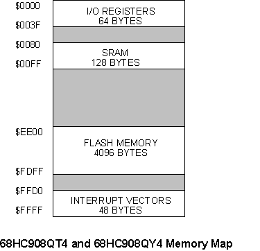
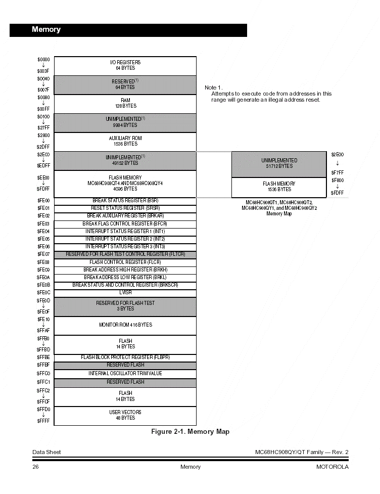
68HC908QY4 Memory Map - Expanded View
Motorola has provided four options for the oscillator on the HC908. These options are:
What more could one ask for? Since we are focussing on low cost embedded applications with the minimum number of components, we are going to select the first option (internal 12.8MHz) for all of our applications. However, in order for the programmer board to work, a stable calibrated oscillator is required to drive the serial communications and programming delay functions. For this reason a 9.8304MHz crystal oscillator is used on the programming board only for the purpose of downloading the code from a PC and programming the target MCU. After programming the MCU will automatically select the internal 12.8MHz oscillator.
The argument over assembler versus C will always arise. Whatever choice you make, consider the following points.
Choosing assembly language programming for the HC908QY4 is highly recommended for the following additional reasons.
The HC908 contains a security feature to make it difficult to read the code of a programmed HC908 MCU. However this security scheme is ineffective. To simplify the programming process the entire flash memory will be erased before programming and therefore the security feature is never utilized.
In order for the programming process to work, the following hardware conditions must be met. These are:
All of these requirements are provided by the programming board. After the target MCU has been successfully programmed these specific inputs are no longer required.
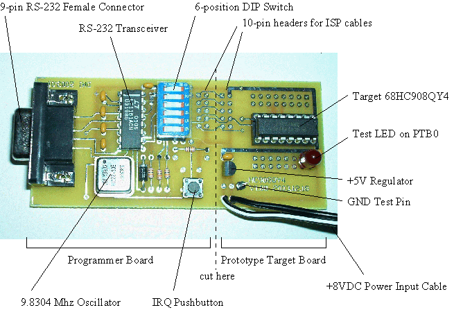
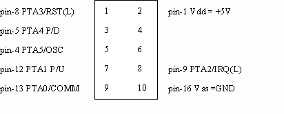
The programming board has provision for installing a 6-position 0.3" wide DIP switch or 0.2" wide jumpers so that you can disconnect/reconnect the following pins on the target HC908QY4 MCU.
|
SWITCH
|
QY4 PIN
|
FUNCTION |
|
1
|
8
|
DTR to RST |
|
2
|
5
|
PTA4 pulled down |
|
3
|
4
|
OSC1 EXT 9.8304MHz |
|
4
|
12
|
PTA1 pulled up |
|
5
|
13
|
PTA0 SCI RXD/TXD |
|
6
|
9
|
IRQ VTST |
When you apply power to the 68HC908QY4 programming/prototype board the MCU may startup in one of two modes.
To ensure that the programmer board starts up in Monitor Mode, before applying power, set SWITCH 1 to OFF and SWITCH 2 to 6 ON. Apply power to the board and then set SWITCH 1 to ON.
After the target MCU has been programmed successfully, press the IRQ pushbutton to run your program.If this fails try setting SWITCH 1 to OFF and then press the pushbutton.
Setting SWITCH 1 to OFF disconnects the serial port DTR line and pulls RTS HI.
Setting SWITCH 6 to OFF (or pressing the pushbuton) removes the 9V Vtst and disables MONITOR MODE.
In normal useage while the MCU is still connected to the programming board, the user program may be started from a POWER-ON RESET. Turn off the power, set SWITCH 1 and 6 to OFF and turn the power on.
(It would be a good idea to plug the 6VDC power-pack into a switched power-bar so that it is easy to turn the power on and off without having to unplug the power-pack.)
If you are using a USB (Universal Serial Bus) to Serial adapter, the programmer may behave differently than when using an ordinary serial port. When the programmer terminates, the DTR (Data Terminal Ready) line is left HI (a LO sends a reset signal to the RST line of the MCU. When using a USB to serial adapter, the DTR line may go LO after the programmer terminates. Setting SWITCH 1 to OFF removes the effect of DTR and the RTS line is pulled HI.
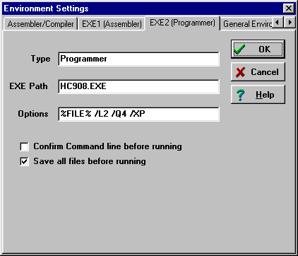
To test that the programmer board and your hookup is working correctly, power up the programming board and connect the serial cable to one of the serial ports of your computer. Open the WINIDE program. Go to Environment menu, Setup Environment... and select the EXE2 (Programmer) screen. Change the assembler options %FILE% /L2 /XP /Q4 to match your serial port, /L1 for COM1 and /L2 for COM2 etc.
Open the sample program called example2.asm and assemble the program by clicking on the Assembler (EXE1) icon. If everything is OK, click on the Programmer(EXE2) icon to download to the programmer.
If everything worked the test LED on the target board will flash continuously once every second.
For more details, please read the next section.
You will need the following:
Set up the hardware as follows:
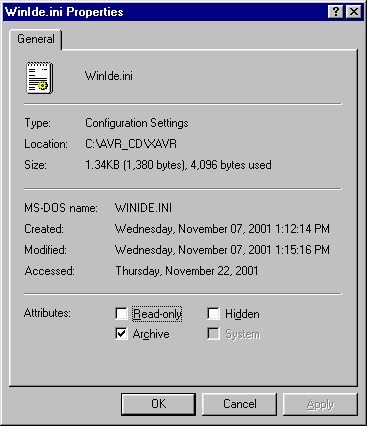
Before starting the WinIDE program, copy the HC908 folder from the CD-ROM to your hard disk. Go to the XAVR folder on your hard disk and right-click on the file called WinIDE.ini. Select Properties and change the Attributes in the WinIDE.ini Properties dialog so that the Read-Only box is disabled. Click OK to dismiss the dialog.
Create a copy of the WinIDE.exe icon and place it on your desktop for easy access.

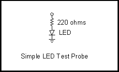
If everything is working you should see the test LED flash at a rate of one flash every second. This confirms that the assembler, cable, downloading process and the MCU is working. You can use the simple LED test probe to observe low frequency pulses on the output pins of the MCU.
If you have access to an oscilloscope, you can begin with example1.asm. This program is the simplest code to test that the downloading process and the MCU is functioning properly. With the oscilloscope you can confirm the correct MCU clock cycle by observing a 167KHz signal consisting of a 2.4us HI pulse and 3.7us LO interval on pins 2 to 15 (except 4, 8, and 9) of the target HC908QY4 MCU.
If an error is detected during the downloading or programming process an error message will be display. Sometimes you may have to try a few times to get it to work.
Whenever one is trying out a new MCU for the first time, it is useful to write the simplest program which will output a pulse on one of the Input/Output pins in a continuous loop. This allows us to do many things such as:
For this you will require an oscilloscope capable of displaying signals of 20MHz or greater in frequency.
The machine code for this program will be stored directly in SRAM and executed from there. Hence no programming of the internal flash memory is required.
The program begins by defining the address of the SRAM and I/O registers used. The assembler pseudo-operations BOOT and ENDB define which parts of the program will be stored in SRAM. All bits of PORTA and PORTB are pulsed thus allowing this program to be used with all HC908 MCUs.
With a XTAL clock of 9.8304MHz, one machine cycle = 4 clock cycles = 0.4069us
The waveform at the output pin should be high for 6 cycles (2.44us) and low for 9 cycles (3.66us) for a total cycle period of 15 cycles (6.10us).
NOTE: Pulses will be observed on pins 2, 3, 5, 6, 7 , 10, 11, 12, 13, 14 and 15 of the 68HC908QY4 MCU. No pulses will be present on pins 4 (OSC1), 8 (RTS) and 9 (IRQ).
|
NOTE that the PTA2/IRQ/KBI2 signal on pin-9 of the 68HC908QY4 is an input only function. |
Example #2 demonstrates one way of testing the HC908 MCU without using an oscilloscope. The output pins are programmed to flash a test LED at a rate of 1Hz. Starting with a XTAL clock of 9.8304MHz, one cycle is 0.407us. This is divided by 64 to give a period of 26us. If the 16-bit timer is set to recycle every 19230 timer count, the timer overflow flag (TOF) would be set every 500ms.
NOTE: Pulses will be observed on pins 2, 3, 5, 6, 7 , 10, 11, 12, 13, 14 and 15 of the 68HC908QY4 MCU. No pulses will be present on pins 4 (OSC1), 8 (RTS) and 9 (IRQ).
(After programming the MCU, do not close the DOS window. Press the pushbutton on the programming board to start the program.)
This performs the same task as Example #2 except that in Example #3 the machine code is programmed into flash memory. The program will therefore run automatically after a power-on reset. The portion of the program delineated by the BOOT and ENDB pesudo-operations is the code called the binary loader program and it is used to burn the flash memory. This part of the code is first loaded in SRAM and then started. The assembler continues the loading process by communicating with the binary loader and transfers the rest of the code, called the object code, to the target MCU.
After the assembler has successfully transfered the object code to the target MCU, the program can be started by pressing the IRQ button. If the MCU is removed from the programming card, the object code will run automatically after a power-on reset.
In this case, the external crystal oscillator is not required and the internal 12.8MHz oscillator is used. Thus one instruction cycle is 0.3125us. When divided by 64 this gives a timer period of exactly 20us. Therefore the timer modulo register is set for 25000 to give a timer period of 500ms.
Eventually, one has to develop techniques for debugging the code in real-time, that is, on the actual target system. Software debuggers, simulators and In-Circuit Emulators (ICE) are extremely useful in tracing code that misbehaves. An oscilloscope is essential in order to view input/output signals. This becomes a necessity in almost every embedded application using small MCUs like the HC908. And last but not least, one must be able to monitor numerical values at different stages of the program. Numerical information can be useful whether it is displayed as binary, decimal, hexadecimal or whatever.
To assist in the debugging process at no extra cost, except for a little extra coding, example4.asm demostrates how to send hexadecimal text to a PC via the COM serial port. Since there is no Serial Communications Interface (SCI) built-in on the HC908, the SCI must be implemented in software using the age-old technique of "bit-banging". This is where an output pin is made to change state to produce the required serial-data bit-stream. This program uses the internal oscillator trimmed to exactly 12.8MHz to produce the serial output at a standard 9600 baud, 8 bits, no parity.
The TERM assembler directive is included in the program. This will invoke a very simple terminal emulator program after the assembly/download process. This allows you to view serial data transmitted from the target MCU for debugging purposes. (The /T option can also be use in the EXE2 assembler command to turn on the Terminal Emulation).
When a blank HC908 MCU is shipped from the factory, address $FFC0, TRIMLOC, will contain a trim value which can be used to set the internal oscillator to the nominal 12.8MHz. To use this value the program would read this location and set it into location $0038, OSCTRIM. Unfortunately the flash memory, including the TRIMLOC is erased to $FF when the MCU is erased prior to reprogramming. The sample program readtrim.asm will allow you to read the value stored at TRIMLOC without erasing the flash memory. The trim value is written in hexadecimal notation to the Terminal Emulator
If the 12.8MHz oscillator frequency is critical, for example when using serial communications, osctrim.asm can be used to observe pulses from PORTB pins on the oscilloscope. The square waveform should have a period of 2ms. Adjust the constant called OSCK until the desired period is obtained.
Use quick.asm to test short parts of a program. In this sample program, code is written to SRAM only and the flash memory is not erased. Serial output uses the external 9.8304MHz oscillator to send data at 9600 baud to the Terminal Emulator. Note that there are only 128 bytes of SRAM and therefore the size of code you can test is limited to this space.
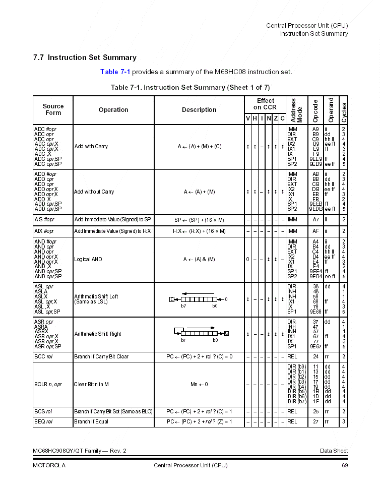
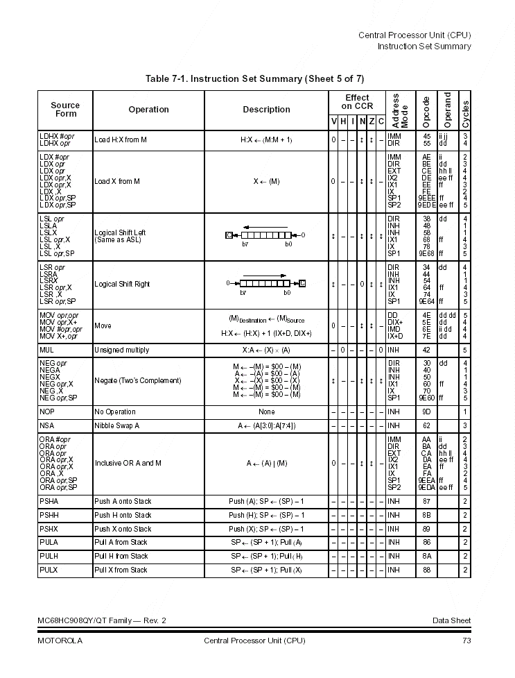
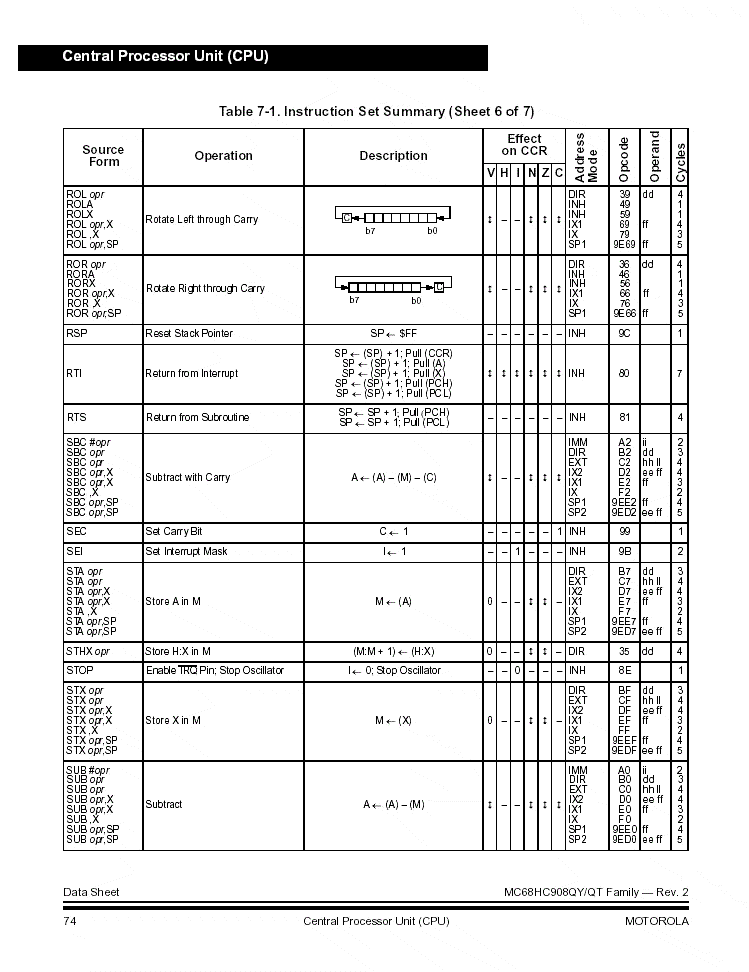
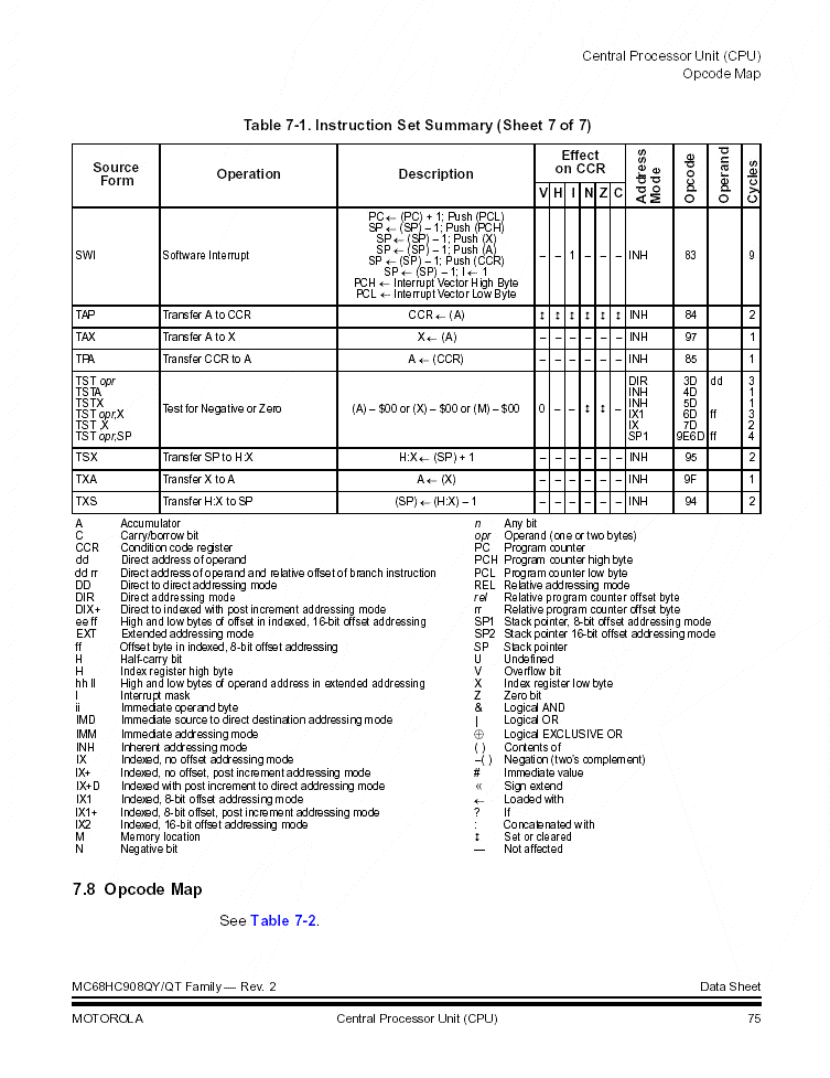
The complete HC908 instruction set is listed here to familiarize you with the HC908 capabilities. For more information, see the HC908 Instruction Table. There are six addressing modes which refer to the different ways parameters are accessed. These modes are as follows:
In the inherent addressing mode, all of the information is contained in the instruction byte. The operands (if any) are registers and no memory reference is required. These are one byte instructions. Here is a list of all the inherent instructions:
| Mathematical Operations | ||
| CLRA | Clear A | |
| CLRH | Clear H | |
| CLRX | Clear X | |
| COMA | 1's Complement A | |
| COMX | 1's Complement X | |
| DAA | Decimal Adjust A | |
| DECA | Decrement A | |
| DECX | Decrement X | |
| INCA | Increment A | |
| INCX | Increment X | |
| NEGA | 2's Complement A | |
| NEGX | 2's Complement X | |
| NSA | Nibble swap A | |
| TSTA | Test A | |
| TSTX | Test X | |
| Shift Operations | ||
| ASLA | Arithmetic Shift Left A | |
| ASLX | Arithmetic Shift Left X | |
| ASRA | Arithmetic Shift Right A | |
| ASRX | Arithmetic Shift Right X | |
| LSLA | Logical Shift Left A (same as ASLA) | |
| LSRA | Logical Shift Right A | |
| ROLA | Rotate Left A | |
| RORA | Rotate Right A | |
| Inter-Register Operations | ||
| TAP | Transfer A to Condition Code Register | |
| TPA | Transfer Condition Code Register to A | |
| TAX | Transfer A to X | |
| TXA | Transfer X to A | |
| TSX | Transfer Stack Pointer to H:X | |
| TXS | Transfer H:S to Stack Pointer | |
| PSHA | Push A onto Stack | |
| PSHH | Push H onto Stack | |
| PSHX | Push X onto Stack | |
| PULA | Pull A from Stack | |
| PULH | Pull H from Stack | |
| PULX | Pull X from Stack | |
| Flag Operations | ||
| CLC | Clear Carry | |
| CLI | Clear Interrupt Mask | |
| CLV | Clear Overflow Flag | |
| SEC | Set Carry | |
| SEI | Set Interrupt Mask | |
| SEV | Set Overflow Flag | |
| Miscellaneous Operations | ||
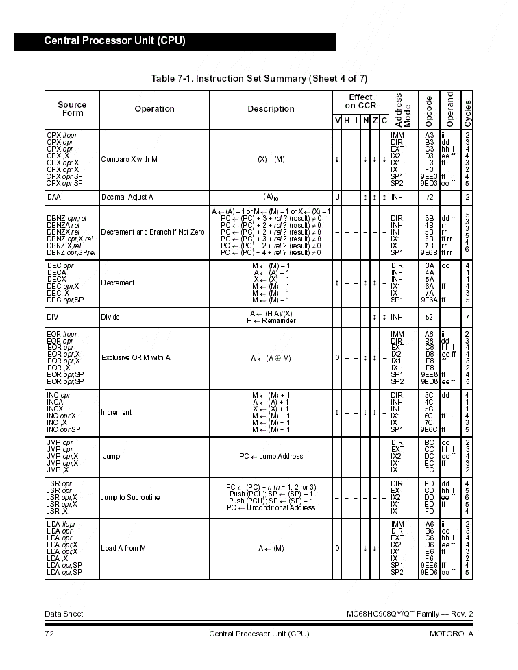
| DIV | Integer Divide (H:A)÷ (X) => A, remainder in H | |
| MUL | Multiply A × X => X:A | |
| NOP | No Operation | |
| RSP | Reset Stack Pointer | |
| RTI | Return from Interrupt | |
| RTS | Return from Subroutine | |
| STOP | Stop Microprocessor | |
| SWI | Software Interrupt | |
| WAI | Wait for Interrupt | |
The HC908 is capable of performing arithmetic and logical operations on memory locations as well as the A and X registers. Thus the programming model is not restricted to the A and X 8-bit registers. This makes implementation of multiple-precision arithmetic possible. For example, it is relatively easy to program the 8-bit HC908 to process 32-bit integers.
|
New for the HC908 are the set of MOV instructions. These instructions allow you to move data from one memory location to another without using the accumulator. While not essential, they obviously simplify the programming task and are a welcome addition to the HC908 set. Examples:
|
In the immediate addressing mode, the actual argument is contained in the byte immediately following the instruction byte. Thus the actual constant value is stored as part of the sequence of bytes that make up the instruction. This mode is selected when the # symbol precedes the argument. Examples:
| LDA | #23 | |||
| LDX | #ONE | |||
| AND | #$F0 |
|
Two new instructions have been added to the HC908 instruction set which are handy when working with the stack pointer and index register. These also help the C compiler when using the stack to store parameters and local variables.
|
In the direct addressing mode (also called page zero addressing) a single byte is used to specify the memory address of the parameter to be accessed. Therefore only addresses $0000 to $00FF are accessible using direct addressing. Instructions using direct addressing are two byte instructions and therefore make more efficient use of machine cycles and memory space. Examples:
| STA | 1 | |||
| STX | RESULT | |||
| LSR | NUM |
In the extended addressing mode, two bytes are required to specify the full 16-bit effective address of the parameter to be referenced. Hence the full range of address from $0000 to $FFFF can be specified. Examples:
| LDA | table | |||
| STX | $FFBE | |||
| JSR | output |
In indexed addressing mode, the index register pair consisting of the H and X register combine to form a 16-bit index register.
|
The 8-bit H-register is new addition to the HC908 programming model. This extends index operations to a full 16-bit index register instead of the older 8-bit X-register. This is a substantial improvement over previous design and it allows index operations to cover the full 64K-byte address range. Note that in order to maintain backward compatibility with previously written 6805 code, the H-register is not automatically pushed on to the stacked when an interrupt occurs. |
In indexed addressing mode, the 16-bit H:X register is used in calculating the effective address. The effective address is the contents of the specified indexed register (X or Y) plus an optional 8-bit unsigned value following the opcode byte. This mode of addressing is useful for accessing individual items or elements of an array or for sequencing through the array. Examples:
| CLR | ,X | ;clear memory at location H:X | |
| INC | 3,X | ;increment location (H:X + 3) | |
| BSET | PORTA X $F0 |
|
The HC908 have added a new group of indexed addressing instructions using the Stack Pointer (SP) as the index register. In this group, a signed 8-bit offset is added to the value of the Stack Pointer to create the effective address. Example,
|
|
The group of memory-accumulator instructions has acquired two new groups of indexed addressing instructions using the Stack Pointer (SP) as the index register. In one case, a signed 8-bit offset is added to the value of the Stack Pointer to create the effective address. The other option is to use an unsigned 16-bit offset added to the Stack Pointer. Example
|
In general, there are two ways to access elements in a table using index address. In the first example below, the address of the table is loaded into the H:X register. Individual elements are referenced by specifying the offset into the table or elements can be accessed sequentially by adding 1 to H:X using AIX #1.
| LDHX | #table | ;load 16-bit address into H:X | |
| LDA | ,X | ;fetch first item in table | |
| ADD | 4,X | ;access 5th item in table | |
| MOV | X+,PORTB | ;access 1st item, increment H:X |
In the second example shown below, the address of the table is specified as the offset and the H:X register contains the index to the table.
| CLRH | ;clear H:X | ||
| CLRX | |||
| LDA | table,X | ;access 1st item in table |
The HC908 does not have an indirect addressing mode. This information is included to round out the discussion on memory addressing modes. Indirect addressing is one of the most powerful and sometimes confusing features available on most computers and yet the concept is fairly simple. With direct (as well as extended) addressing the effective address is specified in the instruction bytes. In indirect addressing mode, the memory location specified by the instruction bytes contains the effective address of the parameter.
In many programming operations, we are not so much concerned about the actual contents of a variable but more about the location of the variable. That is, many times our focus is on the address of a variable and how to manipulate this address. In high level languages such as Pascal and C, structures and pointers rely heavily on the use of indirect addressing. On the HC908, indexed addressing mode is used to implement indirect addressing.
| Memory-Accumulator Operations | ||
| ADC | Add Memory to A with Carry | |
| ADD | Add Memory to A | |
| AND | AND A with Memory | |
| BIT | Bit Test A with Memory | |
| CMP | Compare A with Memory | |
| CPHX | Compare H:X with 16-bit Memory M:M+1 | |
| CPX | Compare X with Memory | |
| EOR | Exclusive OR A with Memory | |
| LDA | Load A with Memory | |
| LDHX | Load H:X with 16-bit Memory M:M+1 | |
| LDX | Load X with Memory | |
| ORA | OR Register A with Memory | |
| SBC | Subtract Memory from A with Carry | |
| STA | Store A to Memory | |
| STHX | Store 16-bit H:X to Memory M: M+1 | |
| STX | Store X to Memory | |
| SUB | Subtract Memory from A | |
| Memory-Only Operations | ||
| ASL | Arithmetic Shift Left | |
| ASR | Arithmetic Shift Right | |
| CLR | Clear Memory | |
| COM | 1's Complement | |
| DEC | Decrement Memory | |
| INC | Increment Memory | |
| LSL | Logical Shift Left (same as ASL) | |
| LSR | Logical Shift Right | |
| NEG | 2's Complement | |
| ROL | Rotate Left | |
| ROR | Rotate Right | |
| TST | Test for zero or minus | |
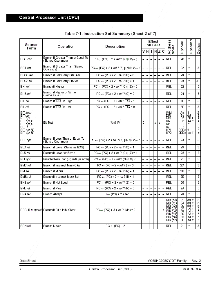
The relative addressing mode is used only for branch instructions. If the branch condition is true, the 8-bit signed integer following the instruction opcode is added to the current contents of the program counter (PC) to form the effective branch address. If the branch is not taken, program execution continues with the next instruction. Examples
| BNE | main | |||
| BSR | putc | |||
| loop | BRCLR | BIT7 PORTB loop |
| Branching - Unsigned Arithmetic | ||||||||||||||||||||||||||||||||||||||||||||||
| BHI | Branch if Higher | |||||||||||||||||||||||||||||||||||||||||||||
| BHS | Branch if Higher or Same (same as BCC) | |||||||||||||||||||||||||||||||||||||||||||||
| BLO | Branch if Lower (same as BCS) | |||||||||||||||||||||||||||||||||||||||||||||
| BLS | Branch if Lower or Same | |||||||||||||||||||||||||||||||||||||||||||||
| Branching - 2's Complement Signed Arithmetic | ||||||||||||||||||||||||||||||||||||||||||||||
| BGE | Branch if Greater than or Equal to zero | |||||||||||||||||||||||||||||||||||||||||||||
| BGT | Branch if Greater Than zero | |||||||||||||||||||||||||||||||||||||||||||||
| BLE | Branch if Less than or Equal to zero | |||||||||||||||||||||||||||||||||||||||||||||
| BLT | Branch if Less Than zero | |||||||||||||||||||||||||||||||||||||||||||||
| General Branching | ||||||||||||||||||||||||||||||||||||||||||||||
| BCC | Branch if Carry is Clear | |||||||||||||||||||||||||||||||||||||||||||||
| BCS | Branch if Carry is Set | |||||||||||||||||||||||||||||||||||||||||||||
| BEQ | Branch if EQual to zero | |||||||||||||||||||||||||||||||||||||||||||||
| BHCC | Branch if Half Carry is Clear | |||||||||||||||||||||||||||||||||||||||||||||
| BHCS | Branch if Half Carry is Set | |||||||||||||||||||||||||||||||||||||||||||||
| BMI | Branch if MInus | |||||||||||||||||||||||||||||||||||||||||||||
| BNE | Branch if Not Equal to zero | |||||||||||||||||||||||||||||||||||||||||||||
| BPL | Branch if PLus | |||||||||||||||||||||||||||||||||||||||||||||
| BRA | BRanch Always | |||||||||||||||||||||||||||||||||||||||||||||
| BRN | BRanch Never | |||||||||||||||||||||||||||||||||||||||||||||
| BVC | Branch if oVerflow is Clear | |||||||||||||||||||||||||||||||||||||||||||||
| BVS | Branch if oVerflow is Set | |||||||||||||||||||||||||||||||||||||||||||||
| BSR | Branch to SubRoutine | |||||||||||||||||||||||||||||||||||||||||||||
| Long Branch | ||||||||||||||||||||||||||||||||||||||||||||||
| JMP | Jump to new location (16-bit address) | |||||||||||||||||||||||||||||||||||||||||||||
| JSR | Jump to SubRoutine (16-bit address) | |||||||||||||||||||||||||||||||||||||||||||||
|
(Technically speaking, these are not relative branch instructions but are absolute jumps using extended addressing mode. These two instructions are listed here to complete the list of branch instructions.) Missing from the group of Branch Instructions are:
In order to test the overflow bit, one will have to transfer the Condition Code Register to register A using TPA and then test bit-7 of register A.
|
||||||||||||||||||||||||||||||||||||||||||||||
Another useful feature of the HC908 is the ability to set or clear any individual
bit of RAM or I/O register using the BSET and BCLR instructions. With the HC908,
unlike the HC11, the BSET, BCLR, BRSET and BRCLR instructions are restricted
to operate on a single bit of the 8-bit target. Also the syntax of the instruction
differs from that of the HC11.
| Bit Set/Clear | ||
| BSET | Bit Set | |
| BCLR | Bit Clear | |
| Branching if Bit Set/Clear | ||
| BRSET | Branch if bit set | |
| BRCLR | Branch if bit clear | |
Examples:
| BSET | 7 NUM | ;set bit 7of NUM | |
| BCLR | BIT3 PORTB | ;clear bit 3 of PORTB | |
| BRSET | 0 NUM MAIN | ;branch to MAIN if bit 0 of NUM is set | |
Alternative Instruction Syntax:
| BSET7 | NUM | ;set bit 7of NUM | |
| BCLR3 | PORTB | ;clear bit 3 of PORTB | |
| BRSET0 | NUM MAIN | ;branch to MAIN if bit 0 of NUM is set | |
16-bit load memory
| LDHX | #1234 | ;load H:X with 16-bit integer | |
| STHX | num16 | ;save in 2-byte num16 |
16-bit increment memory or add to memory
| LDHX | num16 | ;get 16-bit integer | |
| AIX | #1 | ;increment by 1, (-128 to +127) | |
| STHX | num16 | ;store 16-bit integer |
Programs are created using a text editor or any word processor which can produce a text file. The syntax and format for program statements must follow the following rules.
Any text following the semi-colon (;) is treaded as a comment. This style of comment may appear anywhere on the line. An asterix (*) placed at the leftmost position on the line also defines the line as a comment.
| ******************************************************************* | ||||
| * | These are comment lines | |||
| ******************************************************************* | ||||
| ; This also a comment | ||||
| LDA | NUM1 | ;this is a comment after an instruction | ||
Labels or symbols are used for user defined constants, variables, memory addresses and subroutine names. The actual value assigned to the label is expected to be an 8-bit or 16-bit value. The label name may contain upper and lower case letters as well as numerals but no punctuation marks. Label names are case sensitive, for example, PortA and portA are different symbols. Label names should not be more than 10 characters in length.
Labels or symbols are defined when they appear at the leftmost position on the line. The assembler assigns to the label a value that is equal to the current memory address. Labels must not be defined more than once otherwise the assembler will flag an M error, multiple definition attempted. The current memory addess is automatically updated as bytes are occupied, whether for program or data storage.
If the EQU directive is specified then the value appearing in the parameter field, instead of the current memory address, is assigned to the label. The current memory address remains unchanged.
Here are some examples of label definitions:
| FLASH | EQU | $EE00 | ||
| PORTB | EQU | $01 | ||
| bit7 | EQU | %1000000 | ||
| ten | EQU | 10 | ||
| * When deciding which format to use, choose the one | ||||
| * that best describes the object | ||||
| num1 | DS | 2 | ||
| start | LDA | num1 | ||
| ADD | #ten | |||
The assembler can perform limited arithmetic in the expression field. Only a single operation is allowed per expression and the operator must be separated from the parameters by white space. The operators are
| + | add | |
| - | subtract | |
| x | multiply | |
| / | integer divide | |
| % | modulus |
| NUM | DS | 4 | ;reserve 4 bytes for NUM | |
| LDA | NUM | ;fetches MSB | ||
| LDA | NUM + 3 | ;fetches LSB | ||
| * note that the assembler assumes that the first byte reserved is the MSB | ||||
| * followed by the less significant bytes | ||||
BOOT - Defines the start of the binary loader which will be loaded in SRAM. All assembler code following this directive will be placed in SRAM.
ENDB - Defines the end of the binary loader. Assembler code following this directive will be programmed into flash memory. The starting address of the binary loader program is specified in the directive. Example:
| ENDB | .boot |
ORG - Set the assembler's memory address to a new origin.
The ORG directive sets the assembler's current memory address to the value specified in the operand field. If no ORG directive is specified, the memory address is initialized to $0000. Examples:
| ORG | $EE00 | |||
| ORG | FLASH |
END - End of assembly
The END directive indicates to the assembler the end of the program. Any statements following the END directive are treated as comments and are not assembled.
EQU - Equate symbol to a value
The EQU directive assigns the value of the expression in the operand field to the label. The EQU directive assigns a value other than the current memory address to the label. The label cannot be redefined anywhere else in the program. The expression must not contain any forward references or undefined symbols. Examples:
| FLASH | EQU | $EE00 | ||
| ten | EQU | 10 |
FCB - Form Constant Byte (also DB - Define Byte)
The FCB directive stores a byte into the current memory location. Examples:
| CR | FCB | $0D | ||
| ONE | FCB | 1 |
FCC - Form Constant Character
The FCC directive stores a single byte representing the ASCII code the specified character. Examples:
| charA | FCC | A | ||
| quote | FCC | " | ||
| ZERO | FCC | 0 |
Note the differences with the following statements:
| ZERO | EQU | 0 | ;nothing is stored in memory |
| ZERO | FCB | 0 | ;$00 is stored at current PC |
| ZERO | FCC | 0 | ;$60 is stored at current PC |
FCS - Form Constant String
The FCS directive places a sequence of bytes representing the ASCII codes of the characters in the specified string. The first non-space character following FCS is the string delimiter and is not part of the string. The string consists of all characters following the delimiter up to, and not including, the next delimiter. The sequence of bytes stored is terminated with a zero byte. Examples:
| mess | FCS | 'This is a string' |
| title | FCS | $This is another string |
| text | FCS | "The second delimiter is not needed |
FDB - Form Double Byte constant (also DW - Define Word)
The FDB directive places a double byte (16-bits) the the current memory location. The high order byte is placed in the lower of the the memory addresses. Examples:
| num | FDB | 1234 | ||
| vect | FDB | $FFFE | ||
| rstrt | FDB | start |
RMB - Reserve Memory Bytes (also DS - Define Storage)
The DS or RMB directive reserves the specified number of bytes at the current memory address. The memory address counter is then advanced by the specified number of bytes. Examples:
| num | DS | 1 | ;reserve 1 byte |
| result | DS | 4 | ;create a 32-bit result |
| buffer | DS | 16 | ;create a buffer of 16 bytes |
TERM - Invoke Terminal Emulation
The TERM directive will start a simple Terminal Emulation program running on the PC DOS window after the traget MCU has been loaded. This will allow your program to output text information to the PC for quick viewing.
| /L1 | Load using COM1 | |
| /L2 | Load using COM2 | |
| /L3 | Load using COM3 | |
| /L4 | Load using COM4 | |
| /H | Save Intel HEX format object file | |
| /Q2 | Use QT1, QY1, QT2, QY2 memory map (1536 bytes) | |
| /Q4 | Use QT4, QY4 memory map (4096 bytes) | |
| /T | Run Terminal emulation after downloading | |
| /XP | Extra pause after assemblying (for WIN XP) |
| A | Addressing error, relative address is out of range | |
| B | not a Binary character | |
| D | not a Decimal character | |
| H | not a Hexadecimal character | |
| I | Illegal instruction | |
| M | Multiple definition of label attempted | |
| P | Phase error, value of label differs in 1st and 2nd pass | |
| S | Syntax error | |
| U | Undefinded symbol | |
| X | Extended address error, address must be single byte |
2004.10.28
Last Updated 2007.09.07