|
|||
|
Tech
Talk
|
|||
|
Surface
Mount Devices (SMD)
|
So, you were comfortable working with through-hole components in the past. But now you have seen the writing on the wall and the entire electronics industry has gone to surface mount devices (SMD) for various reasons. Your components parts bins are now obsolete and you can no longer get parts in the old DIP (dual in-line plastic) packages. There are a number of good reasons to switch to SMD. For reason #1, the choice was made for you and you have to do it.
1. Your old parts are obsolete and are only available in SMD.
2. Your design will shrink in physical size. You can pack more into a smaller
package or conversely, you need to shrink your design.
3. Your supply voltages will go down and so will power consumption. You no
longer need a huge heat sink or a fan to cool the chips.
4. If you are designing battery operated equipment, your battery will last
longer or you can reduce the size of the battery.
5. With SMD designs it is easy to put a ground plane on the bottom layer,
decoupling capacitors are more compact and leadless, spacing is closer and
the entire noise level goes way down. Your detection limit goes down and signal-to-noise
ratio goes up.
Ok, so you are intimidated by the thought of having to work with SMD. Well, think of the guys who had to switch from vacuum tubes to transistors or from transistors to integrated circuits. This is just another one of those transitions you have to make. So just bite the bullet and do it.
The only intimidating thing about SMD is the overwhelming choices of devices now upon us. It now takes at least four times longer to choose the components for a design. Take, for example, a simple resistor. In the old days before SMD, if I needed a 4K7-ohm resistor, the choice was usually straight forward. An ordinary 4K7 carbon film ¼ watt 5%, yellow-purple-red-gold, would do. The PCB pads would be 0.062 circular with 0.035 holes, 0.400 spacing.
Or as another example, if I needed a quad 2-input AND gate, the choice was simple. An SN74LS08N, 14-pin DIP, 0.100 pitch x 0.300 wide. Done.
Now the choices are overwhelming. You have to choose logic family, supply voltage, power, speed, interface compatibility, temperature range, and finally package.
OK, so let's get started with SMD circuit boards. What do you need?
1. Fine tip soldering iron
2. A second soldering iron
3. Fine solder
4. Solder flux dispenser
5. Tweezers
6. Small Exacto knife
7. Magnifier
8. Anti-static wrist strap
9. Wire-wrap wire
10. Wire-wrap/stripping tool
Explanation and details
1. Soldering iron
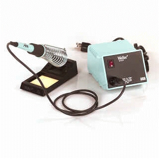 |
The Weller WTCPT Soldering Station is a popular soldering tool with a temperature controlled tip. The PTA7 soldering tip (.062") can be used for normal work. Get the finest soldering tip like the PTS7 with a .015" tip when working with SMD.
|
2. A second soldering iron. Why do you need another soldering iron? Well, this is a research lab, isn't it? You will need to change that SMD resistor or capacitor value. You can get one of those odd shaped soldering tips. But then you have to wait for the soldering iron to cool down before you can change the tips. Better watch out, those tips can give you a nasty burn which is pretty dreadful if you are a guitar player like me.
I keep two soldering irons. One with a very fine PTS7 .015 tip for SMD work and another with a regular PTA7 .062 tip for normal work. To remove an SMD resistor or capacitor, use the soldering irons, one each at both ends of the chip. Commercial boards have SMD components stuck on with glue. Once the solder is melted you have to use a bit of force to get the chip unstuck.
Don't have the right resistor I need in stock? I simply salvage the one I need from an old computer board or hard disk drive PCB. (Techies never throw anything out. You never know when you will need that one component on an old computer board. Like that 2-pin LED connector on the PC mother board. Cut the LED cable with as much wire as you can and save it for a rainy day!)
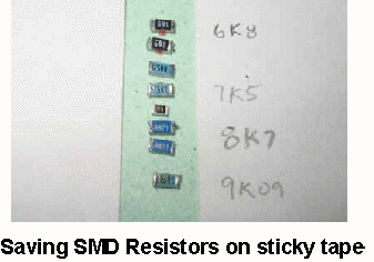 |
What do you do with extra SMD resistors and capacitors? Rather than throwing them away or tossing them into a bin like you would with leaded components, here is a neat trick I use. Take a sheet of plain paper and cut it into two pieces. Take a strip of sticky packing tape and join the two pieces of paper but leave a 1-cm gap of the sticky tape showing in the middle. Now you can stick the SMD chips directly to the sticky tape and write down the value right beside it. You can easily add or remove chips as many times as you wish until the tape is no longer tacky. I have been using my same original "chip carrier" for years now. |
3. Solder
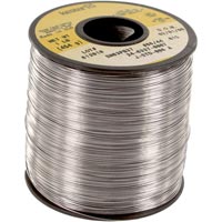 |
You will need small diameter solder for work with SMD. Kester RA Solder "44"in 28 gauge (0.015") will do fine. Note that eventually, all solder will have to be lead free. |
4. Solder flux dispenser
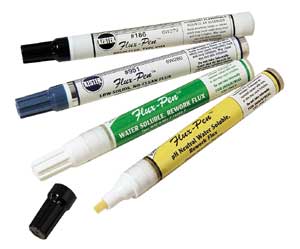 |
Even though the solder has a core of flux, applying a dab of flux on to the SMD pads before soldering allows you to align and tack SMDs and chips on to the PCB before you start soldering. |
6. Magnifier
| If your eyes lack accommodation like mine, you need assistance. Magnifying glasses, Luxo lamps with magnifiers etc. don't work for me. For starters, get one of those magnifying visors that fit around your head. You can pay over $100 for a professional one that the dentists wear, or get one from Princess Auto for $10. This is great for simple visual inspection. |

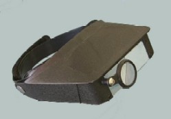 |
Head Magnifying Glass from Princess Auto. |
| For actual soldering work, get a stereo microscope. Magnification of x10 will do. | 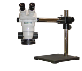 |
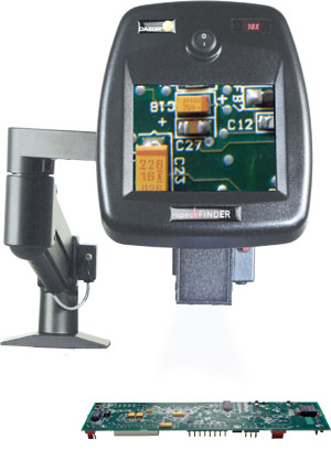 |
If your department can afford it, get the Dazor SpeckFinder for $5000. |
9. Wire-wrap wire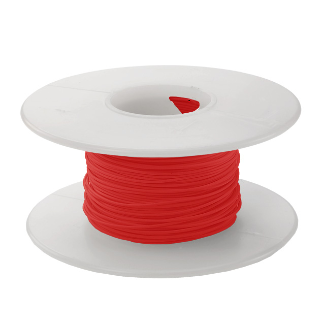
|
Get at least one small spool of wire-wrap wire, size 30 AWG, any colour. You will use this for connecting across the board, fixing up errors, making changes to traces and for those last two traces that were just too difficult to place on the PCB.
|
10. Wire-wrap/stripping tool
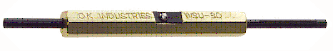
OK Industries WSU-30 tool is used mainly for stripping the insulation off wire-wrap wire.
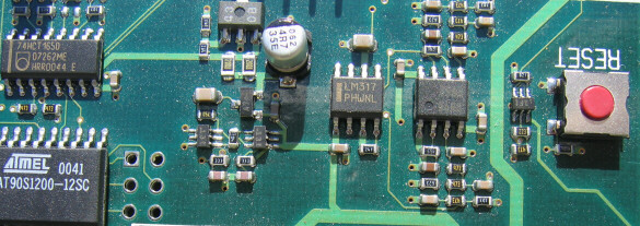
SMD Packagages
The choice of device packages for the same item is now overwhelming. For the purpose of laying out the PCB you have to pay close attention to the package and pin dimensions. In the past, most components could be layed out on a 0.100" x 0.100" grid. Now you have to be comfortable working with both imperial (inches) and metric (millimetres).
For detailed description of package sizes and surface-mount technology (SMT) in general see Wikipedia's SMT pages.
Here is a comparison of the standard DIP package with some standard SMD packaging.
|
Pitch (inches)
|
Width (inches)
|
Pitch (mm)
|
Width (mm)
|
||
| DIP | Dual-Inline Package (leaded) |
0.100
|
0.300
|
2.54
|
|
| SOIC | Small-Outline Integrated Circuit |
0.050
|
1.27
|
||
| SSOP | Shrink Small-Outline Package |
0.025
|
0.635
|
||
| TSOP | Thin Small-Outline Package |
0.5
|
|||
| MLP | Metric Lead-frame Package (no leads) |
0.5
|
|||
For prototyping work, select the SOIC package since it is easier to work with.
It is also easier to patch or make changes to the PCB when necessary.
Avoid using MLP since it is very difficult to solder by hand (but not impossible as I can attest).
SMD resistors and capacitors come in various sizes as follows: