
What is a microcontroller unit (MCU)? An MCU is a complete computer in a single chip. Physical sizes range from a miniscule 8-pin package, 5×5 mm square, to as large as a 30×30 mm square package with 50 to 100 or more pins. MCUs are used in embedded applications meaning that they are used in any application that requires computational power. Applications are widespread, including wristwatches, calculators, telephones, cellular phones, TVs, VCRs, camcorders, dishwashers, microwave ovens, computers, computer equipment, printers, scanners, modems, electronic toys and games, scientific equipment, test equipment, data recorders, industrial controllers, etc. An embedded system is distinct from a personal computer (PC) in that while a PC uses an operating system (OS) such as Windows or Unix to allow the user to run any one of many application-programs, an embedded system is designed to run a single application. It may or may not require an operating system to achieve this. While an MCU may provide a compact and low cost solution to many embedded applications, there are some situations where even a PC (or a single-board PC) may serve as an embedded system. A few examples are POS (point-of-sale) cash register, ATM (automated teller machine), airline reservation terminal, laser printer engine, network server etc.
MCUs come with a variety of features including read-write memory, erasable and non-erasable memory, timers, counters,
real-time clocks, serial interfaces, parallel interfaces, analog to digital converters (ADC), digital to analog
converters (DAC), analog comparators, pulse-width modulation (PWM) outputs, etc. The requirements of the embedded
system obviously depend on the application. For example, a high-speed modem and a compact disk (CD) player both
require high-speed analog recording and data processing. An MCU with digital signal processing (DSP) capabilities
that can perform high-speed numeric computation is essential. On the other hand, a laser printer engine and a network
server both have to handle huge amounts of data and therefore large memories and hard disk drives are required.
The Atmel AVR MCUs compete directly with other popular chips from various manufacturers such as
Where are these chips used? Single chip MCUs are embedded in everyday appliances, instruments, equipment, controllers, data loggers etc., where low size, cost and power consumption are important.
The Atmel AVR family of microcontrollers uses a common core with some variations implemented in over 30 different devices. We will focus our attention on the low cost, small package varieties, in particular, the ATtiny11, ATtiny12, ATtiny15, AT90S1200, AT90S2343, AT90S2313 and AT90S4433.
What are we looking for? In order to focus on specific chips we will be looking at chips with the following properties:
This section summarises the important features of the AVR family. Note that individual MCUs may differ in some areas.
|
ATtiny11 |
ATtiny12 |
ATtiny15 |
AT90S1200 |
AT90S2343 |
AT90S2313 |
AT90S4433 |
|
| Clock Speed MHz |
0-6 |
0-8 |
1.6 |
0-12 |
0-10 |
0-10 |
0-8 |
| Number of pins |
8 |
8 |
8 |
20 |
8 |
20 |
28 |
| Number of I/O pins |
6 |
6 |
6 |
15 |
5 |
15 |
20 |
| RAM |
128 |
128 |
128 |
||||
| EEPROM |
64 |
64 |
64 |
128 |
128 |
256 |
|
| FLASH |
1K |
1K |
1K |
1K |
2K |
2K |
4K |
| On-chip Oscillator |
YES |
YES |
YES |
YES |
YES |
||
| UART |
YES |
YES |
|||||
| 1st Timer |
8-bit |
8-bit |
8-bit |
8-bit |
8-bit |
8-bit |
8-bit |
| 2nd Timer |
8-bit |
16-bit |
16-bit |
||||
| Interrupts |
4 |
5 |
8 |
3 |
2 |
10 |
14 |
| External Interrupts |
1 |
1 |
1 |
1 |
1 |
4 |
4 |
| PWM Output |
YES |
YES |
YES |
||||
| Analog Comparator |
YES |
YES |
YES |
YES |
YES |
YES |
YES |
| 10-bit A/D Channels |
4 |
6 |
|||||
| Input Capture |
YES |
YES |
|||||
| Output Compare |
YES |
YES |
The Atmel AVR MCUs are usually programmed from a host computer such as a desktop PC. Compilers and assemblers are available which will allow you to program in assembly language, BASIC or C. A special programming board, hardware and/or cable is required in order to program your target chip via the PC. This can be in the form of a commercial programmer such as (a) the STK500 from Amtel, (b) a low cost serial programmer from DMI, or (c) a DIY (do-it-yourself) cable that plugs into the parallel port of your PC. No special high voltage is required for programming.
Atmel implements its In-System Programming (ISP) using either a parallel programming mode or a low-voltage serial programming mode. Both EEPROM Data memory and Flash Program memory can be programmed while the MCU is in-circuit. This means that the MCU chips can be directly soldered (DIP or SMD packages) to the printed circuit board and do not require removal for programming or reprogramming.
The serial programming mode uses the Serial Peripheral Interface (SPI). In all, four signals, MISO, MOSI, SCK and RESET are required for serial programming. The DMI serial programmer connects to the RS-232 serial communications port of the host PC and relays the programming commands to the SPI bus of the target MCU.
Programming in BASIC or C has its advantage such as fast software development. However it does come with a price. First of all you have to find a compiler that works. Secondly, code written in BASIC or C always run more slowly and take up more program memory space than the same code written in assembler. All embedded MCU applications involve a lot of bit-manipulation. It is much more efficient from the MCU's perspective if the code is written in assembler. Think twice before using floating-point arithmetic. Libraries required to support floating-point arithmetic take up a lot of memory space.
A PC hosted AVR assembler and Windows IDE (integrated developement environment) is available from DMI for software development in assembly language. Object code is transferred to the target MCU via a single mouse click.
You will need the following:
Set up the hardware as follows:
Before starting the WinIDE program, copy the XAVR folder from the CD-ROM to your hard disk. Go to the XAVR folder on your hard disk and right-click on the file called WinIDE.ini. Select Properties and change the Attributes in the WinIDE.ini Properties dialog so that the Read-Only box is disabled. Click OK to dismiss the dialog.
Create a copy of the WinIDE.exe icon and place it on your desktop for easy access.
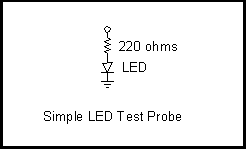
If everything is working you should be able to observe on an oscilloscope a 2MHz signal consisting of a 125ns HI pulse and 375ns LO interval on all pins 12 to 19 of the target AT90S2313 MCU. If you do not have an oscilloscope then repeat the above using the file called example2.asm. This program uses the 16-bit Timer/Counter1 to pulse PORTB at a rate of once every second. Use the simple LED test probe shown below to verify that this is working.
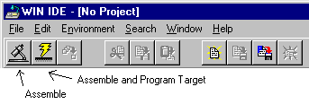
Example #1 shows the simplest program to toggle all the pins on PORTB. This is a simple way to test the WinIDE, Assembler, Programmer and all programming connections. Connect an oscilloscope to any one of pins 12 to 19 of the target AT90S2313 MCU and observe a 2MHz waveform.
Example #2 allows you to test the WinIDE, Assembler, Programmmer and connections using a simple LED logic probe. Connect the LED test probe to any one of pins 12 to 19 of the target AT90S2313 and observe that the LED flashes once every second.
Example #3 demonstrates how to use the serial port to communicate with a host PC. The communications protocol is set for 9600 baud, 8 bits, no parity. Interrupts are not used in this example. Use a terminal emulator program such as HyperTerm (Hypertrm.exe) to test this program. On power up, the AVR MCU should output a message and then echo any characters send from the PC's keyboard.
Example #4 contains subroutines which will allow a program to output text information to a liquid crystal display (LCD). The interface is a common 14-pin connection used by many different LCDs. Here are some examples of compatible LCD modules.
| Manufacturer | Model | Display Format |
| Sharp | LM16255 | 16 characters × 2 lines |
| Optrex | DMC16117 | 16 characters × 1 line |
| Optrex | DMC16207 | 16 characters × 2 lines |
| Optrex | DMC20434 | 20 characters × 4 lines |
Single chip MCUs generally have about 4 working registers or accumulators, namely, an A and B register and perhaps two index registers X and Y. All arithmetic and logic operations are performed using these registers. Motorola's 6805 and 68HC11 family of MCUs are memory based and allow arithmetic and logic operations on memory and input/output addresses just as if they were registers.
The Atmel AVR MCU uses a Harvard RISC architecture with 32 working registers. This architecture is designed for speed. Arithmetic and logic operations are restricted to the registers and are not allowed on memory locations. This has a serious impact on they way we program the AVR MCU. In general, programs written for MCUs in embedded controller applications tend to be small or medium sized. The need for large variable space is not great. This need could very well be accommodated by the 32 registers on the AVR. Therefore the tendency is to dedicate a specific register for a specific variable, for example, a loop counter. Unfortunately, there are some restrictions with the AVR instruction set.
Here is some tips. Registers 0 to 15 are somewhat restricted. Therefore use registers 16 to 25 as your general purpose registers. Reserve registers 26 to 31 for indexed operations. Use registers 1 to 15 for arithmetic functions and data storage. Register 0 is reserved for the LPM instruction. Here is a summary.
| Register | Usage |
| 0 | LPM instruction |
| 1-15 | Math functions and program variables |
| 16-25 | General purpose registers, loop counters |
| 26-31 | Indirect and indexed operations for accessing memory, arrays and strings |
This discussion really only applies to global variables and passing parameters to and from subroutines. Bare in mind that a subroutine can still use any register locally. It is good programming practice to push the register on to the stack before using and restore it before returning from the subroutine using the PUSH and POP instructions.
All instructions are one (16-bit) word in length except the LDS and STS instructions which are two words in length. Instructions are grouped into the following categories:
With inherent instructions, no operand is required since the register that will be affected is implied.
| Operations on the Status Register (SREG) | |||
| CLC | Clear Carry | ||
| SEC | Set Carry | ||
| CLN | Clear Negative flag | ||
| SEN | Set Negative Flag | ||
| CLZ | Clear Zero flag | ||
| SEZ | Set Zero flag | ||
| CLS | Clear Signed test flag | ||
| SES | Set Signed test flag | ||
| CLV | Clear 2's complement overflow | ||
| SEV | Set 2's complement overflow | ||
| CLH | Clear Half carry flag | ||
| SEH | Set Half carry flag | ||
| CLT | Clear T flag (not available) | ||
| SET | Set T flag (not available) | ||
| CLI | Disable global interrupts | ||
| SEI | Enable global interrupts | ||
| Branch Instructions | Alternatives | ||
| IJMP | Indirect Jump PC |
||
| ICALL | Indirect Call PC |
||
| RET | Return from subroutine | RTS | |
| RETI | Return from interrupt | RTI | |
| Miscellaneous | |||
| LPM | Load from program memory R0 |
||
| NOP | No Operation | ||
| SLEEP | Sleep | ||
| WDR | Watchdog Reset | ||
Immediate instructions operate on a single register using a constant value which is part of the instruction. Note that there are restrictions to which registers can be used.
| LDI | reg, K | Load Immediate | registers 16-31 | |
| ANDI | reg, K | AND with constant | registers 16-31 | |
| ORI | reg, K | OR with constant | registers 16-31 | |
| SUBI | reg, K | Subtract constant from register | registers 16-31 | |
| SUBCI | reg, K | Subtract Carry and constant from register | registers 16-31 | |
| CPI | reg, K | Compare register with constant | registers 16-31 | |
| SBR | reg, mask | Set bits in register specified by mask | registers 16-31 | |
| CBR | reg, mask | Clear bits in register specified by mask | registers 16-31 | |
| ADIW | reg, K | Add 6-bit constant to word | register pairs 24, 26, 28, 30 | |
| SBIW | reg, K | Subtract 6-bit constant from word | register pairs 24, 26, 28, 30 |
| PUSH | reg | Push register on to the Stack | ||
| POP | reg | Pop register from the Stack | PULL | |
| LSL | reg | Logical Shift Left | ||
| LSR | reg | Logical Shift Right | ||
| ROL | reg | Rotate Left through Carry | ||
| ROR | reg | Rotate Right through Carry | ||
| ASR | reg | Arithmetic Shift Right | ||
| SWAP | reg | Swap Nibbles | ||
| COM | reg | One's Complement | ||
| NEG | reg | Two's Complement | ||
| INC | reg | Increment | ||
| DEC | reg | Decrement | ||
| TST | reg | Test for Zero or Minus | ||
| CLR | reg | Clear to $00 | ||
| SER | reg | Set to $FF | Registers 16-31 |
| MOV | Rd, Rr | Move | Rd |
|
| ADD | Rd, Rr | Add | Rd |
|
| ADC | Rd, Rr | Add with Carry | Rd |
|
| SUB | Rd, Rr | Subtract | Rd |
|
| SBC | Rd, Rr | Subtract with Carry | Rd |
|
| AND | Rd, Rr | Logical AND | Rd |
|
| OR | Rd, Rr | Logical OR | Rd |
|
| EOR | Rd, Rr | Exclusive OR | Rd |
|
| CP | Rd, Rr | Compare | Rd - Rr | |
| CPC | Rd, Rr | Compare with Carry | Rd - Rr - C | |
| CPSE | Rd, Rr | Compare and skip if equal | skip if Rd = Rr |
These are a powerful group of instructions used to read (load) or write (store) to data memory. Important features to note are:
The SRAM memory or data segment is the assumed memory. The exception to this is the LPM instruction which is used to read a byte stored in the code segment or program memory (flash memory). Since the program memory space is read-only there is no store instruction to write to program space.
The LD and ST instructions use the index registers X, Y and Z. Therefore the listing here only shows the instructions for the Y-index register. The LDD and STD instructions use a memory address which is computed as the contents of the index register (Y or Z) plus a 6-bit (a range from 0 to 63). The LDD and STD instructions are not available with the X-index register. Note that the flags in the status register (SREG) are not affected.
The small versions of the AVR MCU discussed here contain up to 128 bytes of SRAM. Therefore the upper byte of the index register is usually zero.
The LPM instruction is a special case for reading a byte from program space. The Z register is loaded with the 16-bit byte-address. The byte from program space is read into register R0. In this case the upper byte cannot be assumed to be zero. To increment the Z register the following instruction should be used since this operates on the 16-bit register-pair:
ADIW Z, 1
This instruction adds 1 to the R30-R31 register-pair (assuming that Z is declared as R30). The LPM instruction is instrumental in implementing look-up tables, constant strings, arrays and jump tables.
| LPM | Load data from code segment (Z) | R0 |
||
| LDS | reg, label | Load register from SRAM (data segment) | reg |
|
| STS | label, reg | Store (data) SRAM with register | (label) |
|
| LD | reg, Y | Load register from (Y) | ||
| LD | reg, Y+ | Load register from (Y) and increment Y | ||
| LD | reg, -Y | Decrement Y and Load register from (Y) | ||
| LDD | reg, Y + disp | Load register from (Y + disp) | ||
| ST | Y, reg | Store register to (Y) | ||
| ST | Y+, reg | Store register to (Y) and increment Y | ||
| ST | -Y, reg | Decrement Y and Store register to (Y) | ||
| STD | Y +disp, reg | Store register to (Y + disp) |
Input/Output instructions are used to exchange data between a register and an input/output port or to set or clear individual bits of a port.
| IN | reg, port | Input from port | reg |
|
| OUT | port, reg | Output to port | port |
|
| SBI | port, bit | Set bit of port to 1 | ||
| CBI | port, bit | Clear bit of port to 0 |
Note that the SBI and CBI instructions operate on I/O registers $00 to $1F only.
Skip instructions allow the program to redirect the program flow based on the condition of a single bit in a register or input/output port. If the condition is satisfied then the next instruction is skipped. Most often (but not necessarily) the next instruction will be an unconditional branch (JMP) instruction. Note that the flags in the status register (SREG) are not affected.
| CPSE | Rd, Rr | Compare and skip if Rd = Rr | ||
| SBRS | reg, bit | Skip if Bit in Register is Set | ||
| SBRC | reg, bit | Skip if Bit in Register is Cleared | ||
| SBIS | port, bit | Skip if Bit in I/O port is Set | ||
| SBIC | port, bit | Skip if Bit in I/O port is Cleared |
Note that the SBIS and SBIC instructions operate on I/O registers $00 to $1F only.
Branch instructions allow the program to branch to another location (label) if the branch condition is true. This is a relative branch and the range of the destination label is limited to -64 to +63 instructions away from the branch instruction. (The BRBS and BRBC instructions have not been listed below since these two are the general cases for the branch instructions listed below and are never needed.)
| Equivalent mnemonics | ||||
| BREQ | label | Branch if Equal | BEQ | |
| BRNE | label | Branch if Not Equal | BNE | |
| BRCS | label | Branch if Carry is Set | BCS, BLO | |
| BRCC | label | Branch if Carry is Cleared | BCC, BRSH, BHS | |
| BRSH | label | Branch if Same or Higher | BHS, BRCC, BCC | |
| BRLO | label | Branch if Lower | BLO, BCS | |
| BRPL | label | Branch if Plus | BPL | |
| BRMI | label | Branch if Minus | BMI | |
| BRGE | label | Branch if Greater or Equal, signed | BGE | |
| BRLT | label | Branch if Less than, signed | BLT | |
| BRHS | label | Branch if Half Carry is Set | BHCS | |
| BRHC | label | Branch if Half Carry is Cleared | BHCC | |
| BRTS | label | Branch if T flag is Set | ||
| BRTC | label | Branch if T flag is Cleared | ||
| BRVS | label | Branch if Overflow flag is Set | BVS | |
| BRVC | label | Branch if Overflow flag is Cleared | BVC | |
| BRIE | label | Branch if Interrupt is Enabled | ||
| BRID | label | Branch if Interrupt is Disabled |
These instructions are used to redirect the program flow using jumps or subroutine calls.
| Equivalent mnemonics | ||||
| RJMP | label | Jump to label | BRA, JMP | |
| IJMP | Jump to (Z) | |||
| RCALL | label | Call subroutine | BSR, JSR, CALL | |
| ICALL | Call subroutine at (Z) | |||
| RET | Return from subroutine | RTS | ||
| RETI | Reurn from Interrupt | RTI |
Data transfer instructions MOV, LD, LDI, LDD, LDS, LPM, IN, POP etc. do not affect the SREG flags. Therefore
to test the value of a register after a load instruction requires a TST, CP, CPC, CPI etc. instruction to be executed
first before performing a conditional branch.
Never use the actual register number in the instruction, for example,
| MOV | 3 4 | |
| LDI | 16 7 |
This could easily lead to confusion and programming errors. One choice is to define all the registers by names such as the following:
| R0 | EQU | 0 |
| R1 | EQU | 1 |
| R2 | EQU | 2 |
A better idea is to use appropriate variable names such as the following:
| A | EQU | 16 |
| B | EQU | 17 |
| char | EQU | 18 |
| COUNT | EQU | 20 |
| X | EQU | 26 |
| Y | EQU | 28 |
| Z | EQU | 30 |
This makes the program easier to read and also allows you to easily change your register usage without having to check each line of your program. Examples:
| LDI | A 7 | |
| ADD | B A | |
| LDI | Y message | |
| LD | char Y+ |
Remember that the order of the parameters is always
operator destination source
Data movement instructions such as MOV, LD, POP and IN do not affect the flags of the status register (SREG). To test for zero or minus you must use the TST instruction before the conditional branch instruction.
Note that the following instruction is a valid one:
| ADD | A 6 |
But it may not result in what you might expect. This instruction adds the contents of Register 6 to the contents of the register declared as A. There is no ADD Immediate (ADDI) instruction (and this is unfortunate). You could use the following instead but the intent is not so obvious.
| SUBI | A 250 ;since -6 = 256-6 |
Input from a hardware port such as PORTB or PORTD must use the address of the input port such as PINB and PIND.
The instructions SBI, CBI, SBIS and SBIC operate on input/output registers at addresses 0 to 31 only.
MCUs that contain no SRAM space (ATtiny11, ATtiny12, ATtiny15, AT1200) have a severe limitation. Firstly, there is no storage for program variables. Registers have to be dedicated for global variables. A much more severe limitation is that there is no space for a stack. These MCUs utilize a 3-level hardware stack which will severly limit the use of modular programming, that is, nested subroutine calls and storing working registers on to the stack. When using these MCUs, here are points to remember.
When switching from one AVR model to another always double check the I/O register addresses and interrupt vector assignments. These are different from one model to another.
Even though the AVR MCU fetches 16-bit instructions, load and store instructions will only access 8-bit data in and out of memory. The assembler will assign byte-addresses to labels declared in DATA and EEPROM segments. That is, the byte-address is the location of the byte in SRAM or EEPROM.
In CODE segments (program memory space) word-addresses will be generated and assigned to programming labels, except if the label is on a line with one of the following pseudo-op:
FCB, DB, FCC, FCS
FCW, FDB, DW
In these exceptional cases a byte-address is generated and assigned to the label.
A byte-address is the word-address shifted one bit to the left. When a double byte is stored in any segment (FCW, FDB, DW) the assembler will pack the LSB first followed by the MSB. In the CODE segment, the byte-address generated is always even, i.e. bit-0 is set to zero. A byte-address with bit-0 equal to 0 points to the LO-order byte (LSB). A byte-address with a one in bit-0 points to the HI-order byte (MSB). This allows the LPM (Load Program Memory) instructions to be used directly.
For example:
LDI X byte-address
LPM
1. As indicated in the examples above, the AVR syntax specifies the destination operand before the source operand. That is, the format of the instruction is:
operator destination source
2. The XAVR assembler does now allow assembly-time arithmetic such as
LDS A label + 1
For example, on the HC11 it is possible to do the following:
| num | DS | 2 | ;declare num as 2 bytes |
| LDA | num | ;get hi-byte of num | |
| LDB | num + 1 | ;these two can be combined as LDD num |
The XAVR assembler does not allow assembly-time arithmetic. Therefore each byte address of a multi-byte variable must be declared. Since the "dot" is an allowed character, one scheme is shown in the following example:
| D.L | EQU | 18 | ;declare D register lo-byte |
| D.H | EQU | 19 | ;declare D register hi-byte |
| num.L | DS | 1 | ;declare lo-byte of num |
| num.H | DS | 1 | ;declare hi-byte of num |
| LDS | D.L num.L | ;get lo-byte of num | |
| LDS | D.H num.H | ;get hi-byte of num |
3. The XAVR assembler has three new segment declarations DATA, EEPROM and CODE for placing data into the three
memory areas.
4. The XAVR assembler has two new directives LO and HI for generating the LSB and MSB of a byte address.
Ignore this section if you have not used the Motorolal HC11.
|
MC68HC811E2/HC711E9 |
AT90S4433 |
ATmega8 |
|
| Max Clock Speed MHz |
8 |
10 |
16 |
| MIPS (Million Instructions/Second) |
0.5 |
10 |
16 |
| RAM |
256/512 |
128 |
1K |
| EEPROM |
2K/512 |
256 |
512 |
| Program Memory |
0/12K |
4K |
8K |
| Package |
52-pin PLCC |
28-pin DIP, 32-pin TQFP |
28-pin DIP, 32-pin TQFP |
| Number of I/O Pins |
42 |
20 |
32 |
| 1st Timer |
16-bit |
8-bit |
2 × 8-bit |
| 2nd Timer |
16-bit |
16-bit |
|
| Real Time Counter |
1 |
1 |
|
| UART |
1 |
1 |
1 |
| SPI |
1 |
1 |
1 |
| Channels of A/D |
8 |
6 |
6/2 |
| Number of A/D bits |
8 |
10 |
10/8 |
| Analog Comparator |
1 |
1 |
|
| Input Capture functions |
4 |
1 |
1 |
| Output Compare Functions |
4 |
1 |
2 |
| PWM Outputs |
4 |
1 |
3 |
| Hardware Multiply |
YES |
YES |
At the time of writing (Nov. 2001) the Motorola MC68HC811E2CFN2 has been discontinued and has been replaced by the MC68HC711E9CFN2 which comes with 12K OTP (one-time programmable) PROM, 512 bytes RAM and 512 bytes EEPROM. A more fair comparison would be a comparison with the Atmel AT90S81515, AT90S8535, ATmega8 and ATmega16.
Two noticeable advantages the HC11 has over the AVR are:
The advantages of using the AVR over the HC11 are cost, package size and speed.
To a very large extent it is very easy to convert HC11 code to AVR. Most instructions have a direct equivalent. To make life easier, many of the HC11 mnemonics have been retained in the XAVR assembler. For example, BSR, JSR, RCALL and CALL generate the same code on the XAVR.
Here are some examples of direct translations from HC11 to AVR.
| HC11 Syntax | AVR Syntax |
| Immediate Addressing | |
| LDA #$3F | LDI A $3F |
| CMPA #98 | CPI A 98 |
| Direct RAM addressing | |
| LDA num | LDS A num |
| STB num | STS num B |
| Indexed Addressing | |
| LDA 0,Y | LD A Y |
| LDA 1,Y | LD A Y 1 |
| STA 0,Y | ST Y A |
| STB 1,Y | ST Y 1 B |
| Register-register operations | |
| TAB | MOV B A |
| TBA | MOV A B |
| Register Operations | |
| CLRA | CLR A |
| PSHA | PUSH A |
| PULA | PULL A |
| Input/Output | |
| LDA #$FF | LDI A $FF |
| STA PORTD | OUT PORTD A |
| LDA PORTB | IN A PINB |
Note that in general the AVR syntax is: operator destination source
1. Set/Clear Interrupts - This is actually an idiosyncrasy of the HC11 MCU. The HC11 uses an interrupt MASK. Therefore CLI clears the interrupt mask (enables interrupts) and SEI sets the interrupt mask (disables interrupts). With the AVR, SEI enables interrupts and CLI disables interrupts.
2. Unlike the HC11, the LD and ST instructions do not affect the flags in the status register. In order to branch on a zero/non-zero or positive/negative value of a variable loaded from RAM you must use the TST instruction first, for example:
| HC11 Syntax | AVR Syntax |
| LDA num | LDS A num |
| BEQ iszero | TST A |
| BEQ iszero |
3. An input port uses a different address (e.g. PINB) from the output port (e.g. PORTB). Reading the input port reads the actual logic input at the input pins.
4. Arithmetic and Logic instructions are not available on all 32 registers. Registers 16 to 31 are privileged as most instructions apply to these. Reserve these as your general purpose registers. Registers 26-27, 28-29, 30-31 are used for indexed and indirect address and should be reserved for these purposes.
The following instructions are not available on registers 0-15:
LDI CPI ANDI ORI SUBI SBCI SBR CBR SER
5. The instructions CLR (Clear Register) and SER (Set Register) are of questionable value.( Both of these are not
extra instructions in any case since CLR is actually EOR reg,reg and SER is LDI reg,$FF).
6. Skip on register bit set or clear (SBRS, SBRC) can be useful instructions. Unfortunately, the instructions to set and clear register bits (SBR, CBR) do not use the bit-number but use a bit-mask instead. This means that programs have to create constants for both the bit-number as well as the bit-mask. (Note that SBR is the same as ORI in any case). It would have been nicer to have SBR and CBR use a bit-number just as the SBI and CBI instructions.
7. Set and Clear bit in I/O register (SBI and CBI) and Skip if Bit in I/O register is Set or Clear (SBIS and SBIC) operate on I/O addresses 0 to 31 ($00 to $1F) only. You cannot use these instructions on registers involving the timers, input capture, output compare, interrupt flag and mask, MCU control register, watchdog timer and the status register.
8. An ADDI (Add Immediate) instruction is noticeably missing and would be desirable.
9. A LDI (Load Immediate) and CPI (Compare with Immediate) on all registers would have been nice. This would have allowed all of the registers to be usable as general purpose registers.
10. ADIW (Add Immediate to Word) and SBIW (Subtract Immediate from Word) have four idiosyncracies:
11. Register-0 is the implied destination of the LPM (Load Program Memory) instruction.
12. The SBC (Subtract with Carry) instruction does not change the Z-flag if the result of the subtraction is zero. If the result is non-zero the Z-flag is cleared.
|
AVR Serial Programmer Version 1 |
||
|
AT90S2313 Target Board Version 1 |
||
2002.02.15
Last Updated 2007.09.07