| Objectives: To understand the basics of computer hardware interfaces. |
Topics covered:
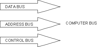
A bus is a common mode of transportation shared by a number of users. This statement is equally true of a computer's bus. In the case of a computer, data is transported from one place to another along a system of wires or connections called the bus. This bus is shared and accessible by many users, that is, the CPU, memory and other peripherial devices.
The bus can be considered to be a collection of three parts, the data bus, address bus and control bus.The data bus is the essential path over which data is transmitted. The purpose of the address bus is to identify the user or the source and destination of the data. For example, every memory location is identified by its memory address. Similarly, every device is assigned an address or range of addresses. The control bus provides timing signals in order to synchronize the transfer of addresses and data, to transack the actual data movement and to provide handshake and bus arbitration information.
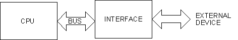
Hardware interfaces are circuits which interact with the CPU via the computer's bus. These are generally printed circuit cards which plug into the interface slots of the computer. Computer interfaces must therefore contain circuits which are able to connect directly to the bus.
There is frequent need to transmit digital information from one device to another over both short and long distances. Serial and parallel interfaces represent two ways of sending information. In parallel transmission, many bits are transferred simultaneously. The primary advantage of this is the increased overall throughput at which information is transferred. This, unfortunately, requires a physical connection for each bit and the extra cabling could become too costly for long distance transmission.
In serial transmission, there is only one data line and information is sent one bit at a time. In effect, the transmission medium is time-shared or time-multiplexed over the number of bits to be sent. This technique, while slower than parallel interfaces, is much more suited to long distance transmissions, particularly when using media such as telephone wires, coaxial cables, radio-frequency waves and fibre optics. Modems, ethernet, USB (Universal Serial Bus), and "FireWire" (IEEE 1394) are all examples of serial interfaces.
Data can be transmitted serially over a single medium or a pair of wires using many different schemes. The most common method of serial transmission is NRZI (non-return to zero - inverted) which has been adopted as the EIA RS-232 standard (a Recommended Standard prepared by the Electronic Industries Association). This is the standard used by the COM1 and COM2 interfaces on your PC.
For transmission over telephone lines, the digital signal must be converted into audio tones using a modulator. At the receiving end a demodulator converts the audio tones back into a digital signal. A modem is a combined unit containing both the modulator and demodulator. When connecting two pieces of equipment using the serial communications port it is useful to observe certain conventions. The data-set or modem is called data communications equipment (DCE). Usually whatever is connected to the DCE is data terminal equipment ( DTE). Therefore the PC is considered to be DTE. This distinction is made because not only is the physical connector different on the two types of equipment but also the function of each signal is reversed.
For DTE, the connector used is a 25-pin male plug designated as DB-25P while the mating socket, DB-25S, would be found on the DCE. A condensed version is also found in the 9-pin DE-9P and DE-9S connectors. The following table shows the signals and pin-numbers for both 9-pin and 25-pin connectors for DTE. The signals' direction and names would change on the DCE connection. In other words, the signal pairs TD/RD, RTS/CTS and DSR/DTR would be interchanged.
|
DE-9 |
DB-25 |
Signal Name | Description as per DTE | |
|
1 |
Protective Ground | |||
|
3 |
2 |
TD | Transmit Data | Signal data from DTE to DCE |
|
2 |
3 |
RD | Receive Data | Signal data to DTE from DCE |
|
7 |
4 |
RTS | Request To Send | Signal from DTE to DCE requesting transmission |
|
8 |
5 |
CTS | Clear To Send | Handshake to DTE from DCE when ready to send |
|
6 |
6 |
DSR | Data Set Ready | Handshake to DTE from DCE when ready |
|
5 |
7 |
GND | Ground | Signal Ground |
|
1 |
8 |
DCD | Data Carrier Detect | Signal to DTE from DCE when carrier present |
|
4 |
20 |
DTR | Data Terminal Ready | Signal from DTE to DCE when ready |
|
9 |
22 |
RI | Ring Indicator | Signal to DTE from DCE when phone is ringing |
Here is a sample RS-232 signal for the ASCII character "M" or 1001101 in binary, for 7-bit data, even
parity (see below) and one stop-bit. Note that the LSB is the first bit to be transmitted following the start bit.
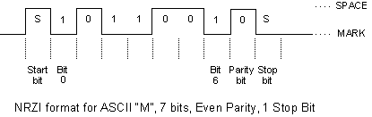
When no data is being transmitted, the condition of the line is in an idle state called mark. This is a carryover from the days of the telegraph when a voltage (actually a current) was transmitted when the key was idle. The start bit is always a single bit duration at a logic level (called space) that is opposite to the mark condition. This identifies the start of the serial bit-stream. The stop bit is the spacing before the next character and is at the mark logic level. This can be 1, 1½ or 2-bit duration. The number of data bits transmitted could differ depending on the particular configuration. The most commonly encountered configuration is 7 data bits plus a parity bit or 8 data bits with no parity.
| It might have been clearer to show the above example drawn inverted. In fact, the NRZI signal is usually drawn with the SPACE level low and the MARK level high. However, the drawing as shown represents the waveform of an actual RS-232 signal that will be observed on the oscilloscope. This is because RS-232 level converters perform the inverting function. |
The rate of change of the signalling medium is measured in units of baud, named after French mathematician Jean Maurice Émile Baudot. Because information bits may be encoded in the signal, the effective data rate could be higher. When the data is not encoded, 1 baud is equivalent to 1 bit per second. Commonly used data rates are 4800 and 9600 baud.
Serial interface cards are readily available which plug into the PC's bus. The purpose of the serial card is to:
A block diagram of a serial interface card is shown.
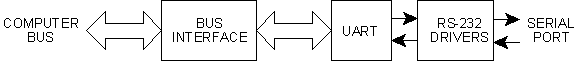
This interface can easily be built using standard 7400 TTL devices. However, LSI devices are available which simplify the design of steps 1 and 2 and reduce the total chip count. Serial communications devices are known by various names by different manufacturers:
With advances in digital technology, ASIC design and increasing demand for low power, compact portable computers, it is now possible to have a number of interface functions in a single chip. For example, Chips and Technologies 82C735 contains two 16550 UARTs, parallel port, floppy disk controller, hard disk IDE interface, mouse and game port all in a single 100-pin package!
Long distance transmission of data is very prone to errors caused by degraded signals, cross-talk, reflections and electromagnetic interference (EMI). Various techniques are implemented to ensure data integrity. One of the simplest techniques is parity checking. The total number of ones transmitted in a collection of bits is either even or odd. If a single bit error had occurred during transmission then the evenness or oddness, i.e. the parity, would be altered. To take advantage of this an extra bit is appended to the transmitted data such that the parity of the combined data is always the same, even or odd. This extra bit is called the parity bit. The choice of even or odd parity is optional as long as the recipient of the data uses the same convention.
This simple error check will detect the occurrence of a single bit error but will not indicate which bit is in error. Secondly, it will not detect the occurrence of an even number of errors.
The ASCII character code is a 7-bit code. Since most computers are byte oriented, eight bits are usually transmitted serially. The most significant bit (MSB) is the parity bit. A commonly used convention in RS-232 serial transmission is a 7-bit data plus even parity. Any program which tests for the occurrence of a particular character must extract the 7-bit ASCII code from the eight bits received. This is accomplished by performing a logical AND operation with a mask, that is, with the binary pattern of 01111111.
Parallel interfaces refer to circuits which allow simultaneous transmission of many bits. Word sizes of 8, 16, 32 and 64 bits are commonly used. Besides the electrical connections for all the bits of the word, there are other connections for control signals used for handshaking purposes. The advantage of parallel interface is the greater through-put possible, i.e., the maximum rate at which data is transferred. Because of the high data rates and the extra cabling required, parallel interfaces are generally limited to short connections under one metre.
The parallel printer port, IDE, SCSI (Small Computer Systems Interface), and GPIB (General Purpose Interface Bus, also known as HPIB and IEEE-488), are examples of parallel interfaces.
The bus consists of data, address and control signals. Since the information on the bus is shared by many different devices, it is constantly changing or time-multiplexed. Hence the information is relevant to a specific device only for a specified instance in time. Furthermore, there are times when the interface will present data to the bus and other times when the interface will accept data from the bus. We can study interfaces to the PC bus by considering output and input functions separately.
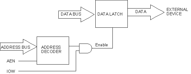
For an output interface, a data latch is required in order to capture the information off the data bus. This latch is clocked when the correct device address is present on the address bus, the address bus is enabled (AEN) and an I/O write operation (as indicated by the presence of IOW) is in progress. This is shown in the block diagram below.
For an input device, data is presented to the bus only at the specified moment. Since the data bus is time-multiplexed between both input and output operations, the bus must be bi-directional. Interfaces can present data only when requested to do so and must disable their output drivers at all other times. This is accomplished with the use of tri-state bus drivers.
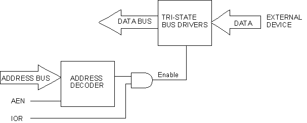
| No two devices must attempt to drive the bus at the same time. Doing so creates a situation called bus contention. |
One can take advantage of LSI (large-scale integration) circuits created to simplify the design of simple parallel input/output interfaces. One such circuit is the Intel 8255 Programmable Peripheral Interface or PPI. This is certainly a large-scale IC with 5800 transistors in a 40-pin package and is equivalent to having three 8-bit interfaces in one package. The PPI provides 24 I/O pins which can be grouped as three 8-bit I/O ports. Each port can be programmed to be an input or output port as desired. A block diagram of a typical interface using the 8255 PPI is show below.
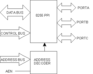
The 8255 PPI is an LSI circuit which simplifies building parallel interfaces to the PC bus. It provides three 8-bit ports which we shall call portA, portB, and portC. These ports are the equivalent of three 8-bit data latches and thus provide you with up to 24 bits of parallel output. If desired, the output of these latches can be disabled and each of the ports can be turned into input ports. Thus, you can choose whether a port is to be an input or an output port.
In actual fact, portC can be considered to be two 4-bit ports which we shall call lower-portC and upper-portC. Each half of portC can be chosen to be input or output, independent of the other half. Included in the PPI is the control logic for decoding and gating the IOR and IOW signals to be used by the rest of the circuit.
The 8255 PPI requires four device address codes in order to access all of its functions. Three addresses allow you to read from or write to the three ports, portA, portB, and portC. A fourth address is used to access a control register. Writing an 8-bit byte into this register defines which ports are to be used as input or output. The format of this control word is shown.
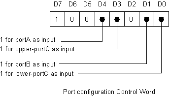
On power up, all ports are configured as inputs, which is the fail-safe mode. Whenever the ports are reconfigured, any ports configured as outputs will output a default logic LO level.
Besides the basic Input/Output mode described, the PPI can be used in two other modes, strobed I/O, and bi-directional bus mode. These two modes will not be discussed here. For more information, see the 8255 PPI Data Sheet.
82C55A Programmable Peripheral Interface Data Sheet (.pdf)
In the laboratory, an interface card containing an 8255 PPI is already built and installed in the PC compatible machines. This card also has the device address decoding circuitry which predefines the PPI at address 344 hex. Thus the four addresses assigned to the PPI are:
| Device Name |
Device Address |
| portA |
344h |
| portB |
345h |
| portC |
346h |
| control word |
347h |
To make interfacing to the PC even simpler, the three PPI ports are routed from the interface card to your breadboard via two 16-conductor cables labelled CABLE 1 and CABLE 4. The pin designations on these two cables are shown, where the bits corresponding to portA are labelled PA0 to PA7, those for portB are PB0 to PB7, and those for portC are PC0 to PC7.
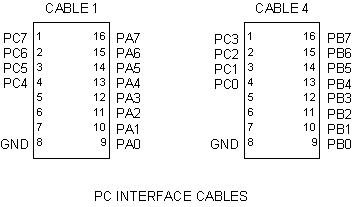
Note that the upper-portC and lower-portC halves are separated on the two cables for a special reason. This is because in a typical application upper-portC would be used as control lines associated with portA and lower-portC would be used in association with portB.
Here is a simplified discussion on the programming of the 8255 PPI. The examples shown make use of the instructions from IBM's BASIC programming language. The basic technique for communicating with an I/O device via BASIC is with the use of the INP and OUT statements:
X = INP(port) 'returns the byte read from a port
OUT port,byte 'sends a byte to a port
The equivalent statements using Turbo Pascal are:
X := PORT[portAddress]; {read the port into X}
PORT[portAddress] := X; {send X to the port}
The default address of the 8255 is 344 hex. Thus, it is convenient to define the addresses of the three ports and the control word as follows:
PORTA = &H344
PORTB = PORTA + 1
PORTC = PORTA + 2
CONTROL = PORTA + 3
First, we have to define whether portA, portB, and portC are to be used for input or output. Remember also that portC can be split into two nibbles. There are 16 possible combinations of portA, portB and portC, in all possible choices of input and output. The combination required is determined by the 8-bit data sent to the control word of the PPI.
For clarity, let us define the following parameters:
AINP = 16
UPPERCINP = 8
BINP = 2
LOWERCINP = 1
Here are some examples of setting the control word:
OUT CONTROL,128 'all ports are outputs
OUT CONTROL,128 + AINP 'portA is input
OUT CONTROL,128 + UPPERCINP 'upper portC is input
OUT CONTROL,128 + BINP 'portB is input
OUT CONTROL,128 + LOWERCINP 'lower portC is input
Combine the control parameters in one statement as in the next example. Suppose we wish portA and upper-portC to be both inputs, with the remaining ports as outputs, we would use the following:
OUT CONTROL,128 + AINP + UPPERCINP
Let us use this last setting in the following discussions. To read the 8-bit input from portA into the variable X, we would write:
X = INP(PORTA)
Also, to read the upper 4-bits of portC into the variable Y, we could use
Y = &HF0 AND INP(PORTC)
Here, we have to mask out the lower half of portC since we had chosen this to be an output port.
In many situations the status of a handshake signal or flag needs to be interrogated by the computer. This signal can be fed to one of the input lines of a port, for example, portC. When reading the value of portC, sound software engineering suggests that you must never assume the inputs of the other unused pins to be at logic zero. Instead, make sure that you mask out all bits except the one that you are interested in and test for a zero or non-zero result. For example:
IF (INP(PORTC) AND $80) <> 0
THEN
ELSE
ENDIF
To send the value of the variable Z (having a value from 0 to 255) to the output portB, we write:
OUT PORTB,Z
If we wish to change a single bit without disturbing the others, we can determine the current state of the output port by reading it. A more elegant way to set or clear a bit is to do the following. Let us define the bit to be changed as BITN (a value from 0 to 7). To set BITN of portB, we could write:
OUT PORTB,INP(PORTB) OR 2^BITN
To clear BITN of portB, we write:
OUT PORTB,INP(PORTB) AND NOT 2^BITN
PortC has been designed such that any of its bits can be set or cleared individually. This is accomplished by writing a special control word to the control register as shown.
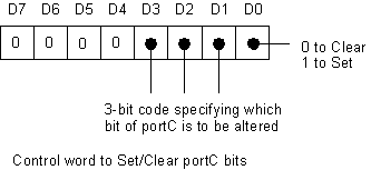
Thus, to clear BITN of portC, use:
OUT CONTROL, BITN*2
To set BITN of portC, use:
OUT CONTROL, BITN*2 + 1
Test the operation of the 8255 PPI as follows. Using a BASIC program, configure portA as output and create a software loop which will toggle the eight bits of portA, HI-LO continuously. Examine the outputs on the oscilloscope.
Use this test as a means of determining the execution time of a typical BASIC instruction.
Test the 8255 PPI for input operations as follows. Using a BASIC program, configure portA as input and enter eight bits from your breadboard switches into the computer. Verify that the data received is correct.
Assume that the address bus consists of an 8-bit address which would allow a total of 256 unique addresses. Design an address decoder circuit which will output a logic HI when the address present on the address bus matches the device address defined by the setting of eight switches.