Chapter 5
Hardware Laboratory
| Objectives: To present rules and guidelines for the hardware laboratory. |
Topics covered:
Rules and Guidelines
The following rules and guidelines must be followed in order to ensure proper care and longevity of equipment
and safety to students.
General Care of Equipment
- Computers and electronic equipment are expensive to acquire, maintain
and repair. Please help us in keeping all equipment in good condition
so that they will be usable for many years to come.
- Learn to use all equipment properly. It is inappropriate to be flicking
knobs and switches without knowing the proper function and usage of
each control. Know what you are doing.
- Ensure that all cords, cables and leads are tidy and without twists,
kinks and undue stress. Always plug and unplug cables and power cords
by firmly grasping the plug. Never pull on the cord.
- Always turn off the power switch on equipment before disconnecting
or connecting to the AC power outlet.
- Report any malfunctioning equipment to the TA or technician immediately.
- Do not move equipment from one work area to another.
- No equipment is to be removed from the laboratory under any circumstances.
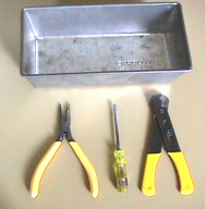
- Each group will be issued the following items at the start of each
lab period:
|
|
|
- Bread-pan
- Needle-nose pliers
- Flat screwdriver
- Wire-stripper
These are to be returned at the end of each lab period.
|
|
|
Working with Breadboards
- Always use the breadboard assigned to you. Do not use another breadboard
without permission.
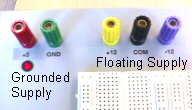
- Some power supplies are grounded, i.e. the zero volt reference is
at safety ground. Others may be floating, i.e. there is no reference
to any ground. In normal usage, connect the COMMON banana-post to the
GND post.
|
|
|
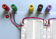
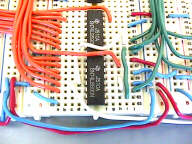
- Connect +5V and GND to vertical rails on the solderless breadboards.
Distribute these to all other vertical rails to create +5V and GND buses.
Use wire of the same colour for all +5V connections, e.g. red, orange
or yellow. Use another colour for GND, e.g. black, brown, green, blue.
|
|
|
- Connect the Vcc and GND pins of the IC to the power bus using short
jumpers. Be consistent with use of colour.
|
|
|
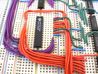
- Make use of coloured wires to differentiate different connections.
|
|
|
- Try to keep all wiring short and tidy and avoid laying wires over
the IC, just in case you have to remove the IC. Make use of colours
to differentiate the signal functions.
|
|
|
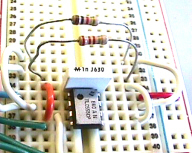
- Do not trim the leads of resistors and capacitors. Arrange them neatly
on the solderless breadboard and connect using short wires.
|
|
|
- The care and safe-keeping of your breadboard is your responsibility. Make
sure you put away your breadboard neatly in your locker at the end of each
laboratory period.
Working with Integrated Circuits and other components.
- All semiconductor components are sensitive to electrostatic discharge
(ESD). While total damage from ESD is more easily detectable, it is
the unseen and undetected weakening of devices that are more costly
in the long run. In electronics assembly plants, the cost to replace
a defective 25¢ component increases exponentially as the product
travels down the assembly line. Eventually, the cost to replace the
same component when the equipment is out in the field can run into thousands
of dollars. Time and money spent in tracing "bugs" and intermittent
and unexpected failures is surprisingly high. Companies concerned with
the reliablility of their products ensure that proper handling procedures
are in place throughout the assembly process.
To reduce the potential for damage from ESD, the following care is
required.
Where provided, make use of anti-static controls and material handling
techniques, i.e., wrist-band grounding straps, anti-static foam and
anti-static bags, grounded workbenches and workstations.
Avoid excessive handling of components, cards, cables, computers, etc.
If you are not wearing a wrist-band grounding strap, discharge yourself
by touching the grounded metal benches in the laboratory before handling
ICs and equipment. This is especially important in the winter after
taking off or putting on any garments, for example, sweaters and coats.
|
|
- Before using an IC, make sure that you identify the proper part number.
In the picture shown, the proper part number is SN74LS139N. The LS stands
for Low power Schottky and the suffix N is the package style, i.e. dual-in-line
plastic (DIP). The letters XAB is the batch code and the numbers
9611 is the date code (11 week of 1996 in this example).
|
|
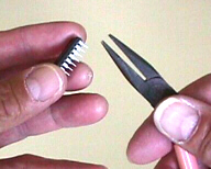
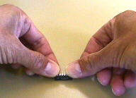
- Check that all the IC pins are straight. If the pins are not straight,
use the needle-nose pliers to straighten them.
|
|
- If the IC is new and never used, straighten all leads on each side
by placing the IC on its side on the bench and press firmly on it in
order to bend the pins to a 90-degree angle.
|
|
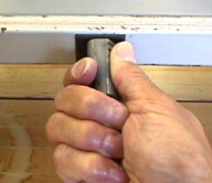
- Do not use your fingers to remove the ICs from the breadboard.
Use the flat screwdriver to gently pry away the IC by alternating at
both ends of the IC. Do not crowbar the IC from one end.
|
|
- Similarly, check the pins on interface cables. Make sure all pins
are straight. If there are any pins missing please notify the lab supervisor
immediately so that a new cable can be provided.
|
|
- Do not pull on interface cables when removing from the breadboard.
Pull on the pull tab instead.
|
|
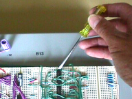
- Connections to the solderless breadboards are made by stripping about
6 mm (¼ inch) of insulation off the end of a length of #22 AWG
solid hookup wire and inserting the bare end into the tiny holes in
the breadboard. Do not use ends that are twisted or bent. Prepare a
fresh end.
|
|
- Occasionally, the end of the wire may break leaving the short bare wire
in the hole. Do not attempt to remove this with the needle-nose pliers.
Doing so will only serve to push the wire futher into the hole and beyond
repair. Please notify the lab supervisor immediately so that the wire
can be safely removed.
- All IC's and components to be used in the lab will be provided and can be
found in the parts drawers. All unused components must be returned to their
proper drawers at the end of the lab period. All components must be returned
at the end of the project.
- All resistors must be returned to their proper drawers. Please read the
colour code and correctly identify the value.
Computer System Design
As with software design, the design of computer hardware systems requires a well planned systematic approach.
A common pitfall of the inexperienced designer is to hastily put together a complex system only to see it fail
on first trial. Trouble shooting the design then becomes a frustrating experience in chaos and the designer has
to go back to the drawing board to start a new design. Proper planning and testing would have prevented this scenario.
A systematic approach to computer system design involves three stages.
- Design
- Implementation
- Testing and documentation
In the first stage the problem must be clearly identified and specifications defined. Examine all possible solutions
to the problem. Both top-down and bottom-up approaches are required. With top-down approach you will develop conceptual
plans of how the solution will be put together. At this stage the design will be void of details of actual implementation,
as with top-down programming.
Applying bottom-up design means that you must be familiar with the specifications and operation of all the devices
to be used in the design.
In the implementation stage, you convert your conceptual design into hardware components. To accomplish this you
will need to examine truth-tables, timing diagrams and device specifications. Rough hand-drawn schematics are approriate
at this stage and must not be overlooked. However, it is important that these drawings be complete logic schematics
with part numbers, pin numbers and signal names. An IC package layout or a physical wiring diagram is NOT appropriate.
As parts of the implementation are put together, they should be tested in isolation. This is the modular approach
to hardware design and testing. Using this technique increases the chances of a working system when all the parts
come together.
Finally, "The job's not over until the paperwork is done!" Your rough schematics must be converted
into proper drawings using either drafting templates or a computer aided design (CAD) program. Complete documentation
will also include a discription of the circuit's operation and its performance, along with truth-tables, timing
diagrams, etc.
Schematic Drawings
There are established standards for drawing circuit diagrams. The sample
schematic is used to demonstrate the following guidelines:
- Draw signal flowing from left to right.
- Junctions are indicated using a dot. U1,7.
- Logic symbols are used and not the IC package layout. U10.
- Pin numbers are placed outside the symbol. U10,11.
- Pin functions are placed inside the symbol. U10,11.
- Label all ICs, e.g. U10.
- Label IC type, e.g. 74177.
- Do not show +Vcc and GND pins except for larger or uncommon ICs.
- All unused inputs should be connected to +Vcc or GND as required. The symbols 1 and 0 may be used as an alternative.
U9,2.
- Negated signals, e.g. RESET, should reflect
the active state condition, i.e. active LO. U6,6.
- Gates should reflect the logic function (i.e. AND or OR) and not the IC type used. Use DeMorgan's theorem.
U5,8.
- Negated outputs, represented by the small circle, should match up with a negated input where ever possible.
U4,11.
- Differentiate between rising edge triggered clocks (U9,3) and falling edge triggered clocks, U10,8.
- Where it is useful show which edge is being used as the trigger source.
A schematic drawing shows the logic function of devices. It is not a wiring diagram.
Here is an example of a badly drawn schematic.
DeMorgan's Theorem
DeMorgan's Theorem provides us with the following two boolean identities:

Because of these identities, it is possible to draw the same logic functions in different ways:
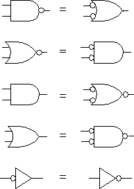
The rule for drawing logic symbols is as follows:
Draw the logic function using POSITIVE logic. That is, if the function is the AND function then show the AND
symbol. If the function is the OR function, show the OR symbol. The bubbles at the inputs and outputs are then
added if the signal is NEGATIVE logic, i.e., ACTIVE-LO.
 For example, do not consider this
as a NAND gate, but an AND gate with an ACTIVE-LO output.
For example, do not consider this
as a NAND gate, but an AND gate with an ACTIVE-LO output.
 Similarly, this is not just an
AND gate, but an OR gate with ACTIVE-LO inputs and an ACTIVE-LO output.
Similarly, this is not just an
AND gate, but an OR gate with ACTIVE-LO inputs and an ACTIVE-LO output.
Do not draw the circuit only on the basis of the IC package. For example, just because the 7408 package is an
AND gate does not mean that you draw the AND gate.
 In this example, the 7474
flip-flop is cleared by either ABORT or CLEAR. Therefore an OR gate is shown even though a 7408 AND gate is used
in the circuit. Note that the clear (reset) function on the flip-flop is ACTIVE-LO.
In this example, the 7474
flip-flop is cleared by either ABORT or CLEAR. Therefore an OR gate is shown even though a 7408 AND gate is used
in the circuit. Note that the clear (reset) function on the flip-flop is ACTIVE-LO.
When analyzing circuit diagrams, it is useful to consider the bubbles not as inverters but as beads on a string.
You can slide the beads along the string without altering the outcome of the logic. When two such beads bump into
each other, they cancel each other.
Introduction to Electronics
This section will review some basic electronic components which you will be using in the laboratory.
Resistors
 The resistance value
and tolerance are identified by coloured bands on the body of the resistor. Resistors in the lab are generally
5%, ¼-watt resistors and will have four coloured bands.
The resistance value
and tolerance are identified by coloured bands on the body of the resistor. Resistors in the lab are generally
5%, ¼-watt resistors and will have four coloured bands.
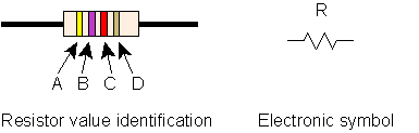
Bands A and B indicate the first and second digits while band C is the multiplier. Thus, the resistance value
is given as AB × 10 C ohms. Coloured band D indicates the tolerance of the resistance
value, i.e., the maximum expected deviation or error from the nominal value.
Resistor Colour Codes
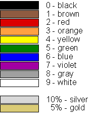 The
numeric value assigned to each colour is shown. Note that the digits from 2
to 7 are the six colours of the rainbow in order. For example, the resistor
shown in the photograph with colour bands of yellow-purple-red-gold indicates
a 4700 or 4.7k, 5% resistor. In international notation, this value is shown
in schematics as 4k7 where the multiplier (k) replaces the decimal point. This
notation avoids error from an obscure decimal point.
The
numeric value assigned to each colour is shown. Note that the digits from 2
to 7 are the six colours of the rainbow in order. For example, the resistor
shown in the photograph with colour bands of yellow-purple-red-gold indicates
a 4700 or 4.7k, 5% resistor. In international notation, this value is shown
in schematics as 4k7 where the multiplier (k) replaces the decimal point. This
notation avoids error from an obscure decimal point.
Standard Resistance Values
| 1.0 |
1.2 |
1.5 |
1.8 |
| 2.2 |
2.7 |
3.3 |
3.9 |
| 4.7 |
5.6 |
6.8 |
7.5 |
| 8.2 |
9.1 |
|
|
Multiply these values by any multiple of 10 to arrive at standard values for 5% resistors. These values are
approximately 20% apart.
An interesting note on tolerances
It can be beneficial for electronic companies to periodically check on the quality control of component manufacturers.
Suppose that the resistance values of 1000 resistors, with a nominal value of 100 ohms, taken from the same batch
of resistors were measured and tabulated. One can expect a distribution of resistance values centered about the
nominal value. Here are some typical histograms showing different distributions.
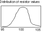
In this distribution, the values are well within the ±5% tolerance limits.

Here the manufacturer has good process control and manages to keep the tolerance to ±2%.

While these values still meet the specified tolerance, this shows that the manufacturer is experiencing some
process control problems.

Here the manufacturer has poor process control and relies on measurement to reject resistors falling outside
of the 5% tolerance limits.
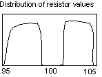
Worst of all, this manufacturer sorts and removes the 1% resistors which can then be sold at a higher price.
Variable Resistors
Variable resistors are also commonly known as potentiometers or pots for short. These are used to provide
output voltage Vout as a variable fraction of an input voltage in a circuit called a potential divider.
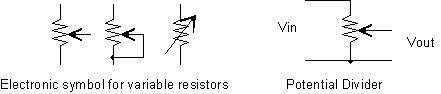
They can also be used to provide a variable resistance which will allow fine tuning of frequencies, time delays,
RC constants, etc. Note that every pot comes with three terminals. The centre terminal is usually the slider or
wiper arm which provides the variable contact along the body of the resistor.
Capacitors
 The standard unit of capacitance
is the Farad. However, 1F is a huge value. Non-polarized disc capacitors are commonly available in the range
10pF to 1µF. These are used in timing and frequency dependent applications such as RC circuits and filters.
The capacitance value may be printed on the capacitor in a number of ways:
The standard unit of capacitance
is the Farad. However, 1F is a huge value. Non-polarized disc capacitors are commonly available in the range
10pF to 1µF. These are used in timing and frequency dependent applications such as RC circuits and filters.
The capacitance value may be printed on the capacitor in a number of ways:
- value in pF, e.g. 4700 = 4.7nF
- value in µF, e.g. .022 = .022µF = 22nF
- value as per resistor code, e.g 104 = 100nF = 0.1µF
- value as per international code, e.g. n15 = 0.15nF = 150pF
(micro = × 10-6, nano = × 10-9, pico = × 10-12)
With familiarity, you will learn to identify the proper value judging from the physical size of the capacitor.
 Electrolytics are polarized and must
be inserted into the circuit with the negative lead towards the more negative potential. The negative lead is identified
by the -ve sign or the arrow. These capacitors are commonly used in power supplies, large RC timing and DC blocking
and are available in much higher values than discs, ranging from 1µF to 10,000µF.
Electrolytics are polarized and must
be inserted into the circuit with the negative lead towards the more negative potential. The negative lead is identified
by the -ve sign or the arrow. These capacitors are commonly used in power supplies, large RC timing and DC blocking
and are available in much higher values than discs, ranging from 1µF to 10,000µF.
 "Super-caps"
with values such as 1F are now available. Capacitors of these values are more likely to be used as batteries!
"Super-caps"
with values such as 1F are now available. Capacitors of these values are more likely to be used as batteries!
Oscilloscopes
Just as a programming language debugger allows you to follow the inner workings of a program, an oscilloscope
is your window into the inner workings of the hardware. It is therefore important that you become comfortable as
well as competent in the use of the oscilloscope.
Sometimes a simple light indicator or light emitting diode (LED) might be used to monitor output levels. The
oscilloscope, however, is far superior, whereas an LED can be misleading at times. In particular, an LED will not
indicate the following conditions:
- A high frequency oscillation.
- A floating input or output.
- A glitch or very small spike.
- An output with insufficient drive (a low HI).
- An output with insufficient current sinking ( a high LO).
- A noisy signal.
- A signal with ringing on the rising and falling transitions.
- A signal with instability at the transitions.
- A delay between signals.
Furthermore, the oscilloscope allows you to make precise time and voltage measurements. For these reasons and
many others it is important to use the oscilloscope at all times when testing and debugging circuits and associated
systems.
Getting Started
First, you must become familiar with the usage and settings of all the controls of the oscilloscope. The controls
are identified by the numbers shown and described below. Go over all the controls and make sure that you understand
their functions.
Picture of Tektronix Model 2213, 2213A
and 2225 oscilloscope.
| BEAM CONTROL |
|
| 1 INTENSITY |
Controls trace brightness |
| 2 BEAM FIND |
Locates the beam if off the screen |
| 3 FOCUS |
Focuses the beam |
| 5 POWER |
ON/OFF Power switch |
| 6 Power Indicator |
Light comes on when POWER is ON (2225 only) |
| |
|
| VERTICAL CONTROL |
|
| 7 CH1 POSITION |
Channel 1 vertical position control |
| 9 CH2 POSITION |
Channel 2 vertical position control |
| 10 CH1-BOTH-CH2 |
Selects CH1, CH2 or BOTH |
| 11 NORM-INVERT |
Inverts Channel 2 when depressed |
| 12 ADD |
Sum of CH1 and CH2 is displayed |
| ALT |
Beam alternates between CH1 and CH2 |
| CHOP |
Beam is rapidly switched between CH1 and CH2 |
| 13 CH1 & CH2 VOLTS/DIV |
Vertical gain or sensitivity |
| 14 CAL |
Rotary knob must be in indented position for calibrated vertical scales |
| 15 AC |
Only the AC component displayed |
| GND |
Shows zero volt reference line on the screen |
| DC |
DC and AC components are displayed |
| 16 CH1 & CH2 INPUT |
BNC input jacks for CH1 and CH2 signals |
| |
|
| HORIZONTAL CONTROL |
|
| 17 COURSE POSITION |
Course horizontal adjustment |
| 18 FINE POSITION |
Fine horizontal adjustment |
| 19 X1-ALT-MAG |
|
| X1 |
Normal (unmagnified) waveforms |
| ALT |
Alternating display of normal and magnified waveforms |
| MAG |
Magnified waveforms |
| 20 SWEEP (SEC/DIV) |
Horizontal sweep rate, i.e. horizontal scale |
| 21 CAL |
Must be in CAL position for calibrated horizontal scale |
| 21 x10 |
When pulled out, the sweep rate is magnified by 10 (2213 only) |
| 22 x5-x10-x50 MAG |
Horizontal magnification (2225 only) |
| |
|
| TRIGGER CONTROL |
|
| 25 SLOPE |
Selects rising or falling trigger source |
| 26 LEVEL |
Selects the trigger threshold level |
| 27 TRIG'D |
Light shows when the horizontal sweep is triggered |
| 28 MODE |
|
| AUTO |
Triggers automatically at preset levels |
| NORM |
Triggers when the threshold level is exceeded |
| TV FIELD |
Triggers from television field signals |
| SGL SWP |
Triggers once only at threshold level |
| 29 RESET |
Used to reset and arm trigger for SGL SWP |
| 30 HOLDOFF |
Varies the time delay before the next horizontal sweep |
| 31 SOURCE |
Selects CH1, CH2, LINE frequency or EXTernal trigger source |
| 32 COUPLING |
Selects AC or AC & DC trigger signal |
| 33 EXT INPUT |
BNC connector for external trigger signal |
Home Problems Next Chapter