| Objectives: To demonstrate various concepts of assembly
language programming and development using the HCS08. |
Topics covered:
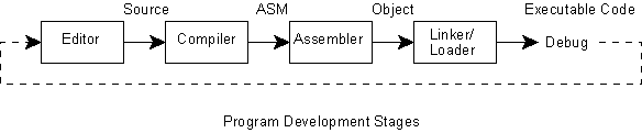
The traditional way of developing a program written in assembly or high level language such as C is to begin with an editor in order to create a text file. This file is converted by a source code compiler to produce object code. Finally, the object code is linked, loaded and then executed. In some cases, the compiler first converts the source code to an assembly language file and then an assembler converts the assembly code into object code. This stage is usually hidden from the programmer. The entire process can be viewed graphically as shown.
Running and debugging of the program may be performed on a code simulator or can take place directly on the target MCU. When errors in programming have been detected, the source code has to corrected and the entire process must be repeated. Programming today has been improved and made a more efficient process with the use of an integrated development environment (IDE) where the entire task of editing, compiling, linking, loading and debugging is streamlined from within a single program.
The letters of the alphabet, digits and punctuation marks are collectively called alphanumeric characters. The American Standard Code for Information Interchange (ASCII, pronounced "askee") is a 7-bit code used to represent a standard set of alphanumeric characters. This code can represent 128 characters of which only about 96 are required for alphanumeric characters. The remaining codes are used for special purposes such as line-feed, return, bell, etc., which are usually not visible or printable. These are called control characters. (Control characters are generated on the keyboard by holding the Ctrl key down and then pressing another key).
The 48th character (starting with the zeroth as the first) in the ASCII table is the character "0" and progresses to "9" as the 57th character. The letter "A" is the 65th character and so on.
The smallest group of bits handled by most computers is 8 bits, that is, a byte. With one byte it is possible to represent 256 characters. Many personal computers use an extended ASCII, making use of the extra 128 codes to represent special graphic symbols originating with the IBM PC. In order to accommodate other languages, including Chinese and Japanese, a 16-bit representation called Unicode is rapidly becoming the new standard.
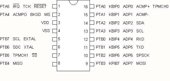
The drawing above shows the pin designations of the MC9S08QG8. Besides the power connections VDD and VSS (GND), there are 14 general purpose input/ouput pins, PTA5-PTA0 and PTB7-PTB0. Parallel interface refers to a data transfer mechanism where data is presented to a number of data lines simultaneously. The advantage of this is data can be transferred at the fastest rates but has the disadvantage that it requires N physical connections to transfer N bits at a time.
Serial interface refers to a data transfer mechanism whereby data is transmitted over a single wire, one bit at a time. A simple analogy is like having a single lane roadway versus a multiple lane highway.
The HCS08 comes with a full-duplex asynchronous Serial Communications Interface (SCI) which is used to communicate with other computers and devices via a two-wire interface, transmit data TXD, received data RXD, plus signal ground GND. When the SCI is enabled, MC9S08QG8 MCU pin-11 becomes TXD and pin-12 is RXD. Voltage levels of TXD and RXD are at the MCU TTL (transistor-transistor logic) levels. A standard specification of timing and voltage known as RS-232 is commonly used in the computer industry for communicating between various computers and peripherials such as printers, scanners and modems. This has virtually been superseded with the Universal Serial Bus (USB) which is essentially a two-wire interface (complementary data lines at 0-5V levels) plus 5V power and GND, not unlike another standard called RS-485. When the RS-232 standard is required, a special transceiver interface chip (such as the MAX232) is used to convert from TTL levels to RS-232 levels.
What can the SCI be used for? The SCI is a simple asynchronous mechanism for transferring commands or data from one MCU to another MCU or PC, or an external peripheral such as a printer. It could also be used to communicate between devices using radio-frequency (RF) wireless waves, infra-red (IR) or fiber optics.
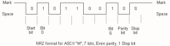
The diagram below shows a typical voltage waveform for the 77th character in the ASCII table. The 7-bit data transmitted is 1001101 in binary or 4D in hexadecimal and is used to represent the letter "M". Data transmitted via the SCI can be 7, 8 or 9 bits. In addition, a start-bit, parity-bit and stop-bit are appended to the data. Two common communications protocols are 7 bits, even parity and one stop-bit (7E1) and 8 bits, no parity and one stop-bit (8N1).
For baud rates to be accurate, the internal oscillator must be set as closely as possible to 16MHz. This is done by setting the Internal Clock Source Trim register ICSTRM. One way of determining the appropriate value to use is to let Debug determine this for the first time and then manually read the setting that Debug has chosen. To do this, run your program using IC Debug mode and perform the following steps:.
Now use this value in your main program to set ICSTRM. You may have to tweak this value to arrive at the correct clock frequency.
Setting up and using the SCI is fairly straight forward.
See the MC9S08QG8 Data Sheet, Chapter 14, SCI.
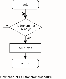
To initialize the SCI, set the baud divider for 9600 baud by writing 0 to SCIBDH and 26 to SCIBDL. Enable the SCI receiver and transmitter by writing 00001100 ($0C) to SCIC2. Before transmitting each character, the Transmit Data Register Empty flag (TDRE) in register SCIS1 must first be checked to make sure that it is set. This can be done using a classic polling mechanism as illustrated in the following flow chart.
Transmit a byte by storing the byte to the SCID register.
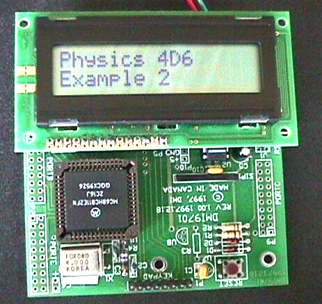
The HC11 demo board comes with a 2-line by 16-character Liquid Crystal Display (LCD) and has been programmed to accept SCI signals, either TTL or RS-232 levels. This can be used as a simple display terminal or for debugging your MCU code. The HC11 will accept standard 7-bit ASCII characters at 9600 baud, 8-data bits, no parity, one stop-bit. The following special control characters will perform the actions shown.
| Hex | Function | ||
| 01 | Home to start of line #1 | ||
| 02 | Home to start of line #2 | ||
| 03 | Clear Screen | ||
| 08 | Backspace - move cursor back one position | ||
| 0A | Line Feed - move cursor to next line | ||
| 0D | Carriage Return - move cursor to start of current line | ||
The modulo timer subsystem is a simple 8-bit timer/counter which can be used to implement simple hardware timers or counters. The timer input clock can come from various sources and the frequency can be divided by powers of 2. For example, to set the divider to 256, write $10 to MTIMCLK. Start the timer by writing $00 to MTIMSC. The value of the timer can be read from register MTIMCNT. To clear the timer count, write a 1 to bit-5 of MTIMSC.
The timer overflow flag TOF can be read from bit-7 of register MTIMSC.
For more information on the Modulo Timer, see the MC9S08QG8 Data Sheet, Chapter 13, Modulo Timer.
Hardware interrupts are very important features of computers. Computer instructions are executed in a linear fashion. That is, instructions are fetched and executed one after another. While it is possible for the program to take different paths, only one task can be accomplished at any instance in time. Multi-tasking, the resemblance of performing many tasks at the same time, is in fact the CPU rapidly switching from one task to another. The CPU still performs one task at a time.
Interrupt is the mechanism for pre-empting the attention of the CPU so that another task can be dealt with, just as you may be called away from your work temporarily when the phone rings. In a multi-tasking operating system, a periodic timer interrupt can be used in order to perform many different tasks in round-robin fashion. Interrupts are also used when a high priority event must be dealt with in a timely fashion.
In all cases of interrupts, the flow of instruction execution is abruptly suspended. The new task is performed and then program execution resumes at the point where it was interrupted. For all of this to happen in a smooth manner, the CPU (and software) must be capable of two things. Firstly, the CPU must record the address of the next instruction to be executed at the moment of interruption. This is the only way that the CPU would be able to resume proper program execution once the interrupting task was dealt with. Secondly, the context of all resources, i.e., accumulators, registers and flags, must be saved since these could be altered by the interrupting tasks.
On the HCS08, this is automatically taken care of by the CPU when an interrupt occurs. The current program counter, accumulators and flags are stored on the stack (also covered in Chaper 4) before the interrupt is serviced.
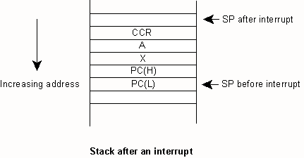
The first pair of bytes to be pushed on to the stack is the current contents of the program counter, which would be the address of the next instruction to be executed. This is followed by the X index register, A accumulator and Condition Code Register. The PC is then loaded with a new address which is the address of the interrupt service routine (ISR) taken from the interrupt vector table. (Note that for backward compatiblity with previous HC08 processors the H register is not saved on the stack).
At the completion of the ISR, the RTI (Return from Interrupt) instruction is executed. This instruction pops all the registers off the stack in reverse order so that the context of the CPU is restored to the state that it was at the time of the interrupt.
The HCS08 is designed to handle interrupts from 32 different sources. This is accomplished by reserving the last 64 bytes of program memory space from address $FFC0 to $FFFF called the interrupt vector table. For each interrupt, a pair of bytes in the table is used to store the address of the ISR. Here are the assignments for interrupt vectors that are available.
|
Vector Number
|
Vector Address |
Interrupt Source |
|
23
|
FFD0-FFD1
|
Real-time interrupt |
|
22
|
FFD2-FFD3
|
|
|
21
|
FFD4-FFD5
|
|
|
20
|
FFD6-FFD7 |
ACF - Analog Comparator |
|
19
|
FFD8-FFD9 |
COCO - Analog/Digital Converter |
|
18
|
FFDA-FFDB |
KBF - Keyboard interface |
|
17
|
FFDC-FFDD |
IICIF - IIC interface |
|
16
|
FFDE-FFDF |
TDRE - SCI transmit |
|
15
|
FFE0-FFE1 |
RDRF - SCI receive |
|
14
|
FFE2-FFE3 |
SCI error |
|
13
|
FFE4-FFE5 |
SPIF - SPI |
|
12
|
FFE6-FFE7 |
TOF - Modulo Timer |
|
11
|
FFE8-FFE9 |
|
|
10
|
FFEA-FFEB |
|
|
9
|
FFEC-FFED |
|
|
8
|
FFEE-FFEF |
|
|
7
|
FFF0-FFF1 |
TOF - TPM overflow |
|
6
|
FFF2-FFF3 |
CH1F - TPM channel 1 |
|
5
|
FFF4-FFF5 |
CH0F - TPM channel 0 |
|
4
|
FFF6-FFF7 |
|
|
3
|
FFF8-FFF9 |
LVDF - Low-Voltage Detect |
|
2
|
FFFA-FFFB |
IRQF - IRQ pin |
|
1
|
FFFC-FFFD |
SWI - Software Interrupt |
|
0
|
FFFE-FFFF |
RESET |
Interrupt latency is the time taken from the onset of the interrupting event to the start of the interrupt service routine. This includes the time taken for the CPU to respond to the interrupt, finish executing the current instruction, save the registers on to the stack, and fetch the ISR address from the interrupt vector table. The interrupt service time is the time taken by the ISR to service the interrupt, that is, the length of time occupied by the ISR. The total interrupt response time is the sum of the interrupt latency and the service. This is a measure of how rapidly the system responds to interrupts and therefore the maximum allowable rate of interrupts.
In order to achieve the fastest response, it is important that all interrupt service routines be executed as quickly as possible. Therefore ISR tasks should be restricted to simply acknowledging and dismissing the interrupt flag. Any involved tasks or calculations should be done outside of the ISR.
| A Mac student riding a bicycle is struck down by an automobile. Someone calls for an ambulance which arrives on the scene in two minutes. By the above definition, the ambulance's latency is 2 minutes. The student is in critical condition and the paramedics do only what is absolutely essential before rushing to the hospital. The time spent providing essential care and transportation to the hospital is 8 minutes, which we call the service time. The total response time is 10 minutes, during which time the ambulance is tied up and cannot respond to another incident. |
In order to properly implement interrupts on an HCS08 MCU the following four steps must be taken.
CodeWarrior for HCS08 will make Steps 1 and 2 very straight forward. Create an ISR template in C using the following as an example.
| // example of ISR for Modulo Timer Overflow | ||||
| void interrupt 12 TimerISR() | ||||
| { | ||||
| asm | ||||
| { | ||||
| } | ||||
| } | ||||
The compiler directive interrupt 12 informs the compiler that this is your ISR whose starting address is to be placed at interrupt vector location #12. The name of the ISR can be any name of your choosing. The compiler will automatically terminate the ISR with the RTI instruction. In your ISR, make sure that the interrupt is serviced by clearing the interrupting flag.
Step #3 and Step #4 should be performed at the start of your main procedure.
MC9S08QG8 Data Manual, 300 pages, 3Mb pdf
MC9S08QG8 Instruction Set Summary