5. Analogue-to-Digital Conversion
5.1 Parallel Converter
An extremely important procedure currently dominating much of signal analysis is the conversion of analogue
information into digital data. A variety of arrangements have been developed to accomplish this transformation.
The simplest is the parallel or 'flash' ADC. The signal v(t) is sent to 2N-1 comparators. The reference
input is generated from a common reference voltage, employing a chain of 2N resistors.
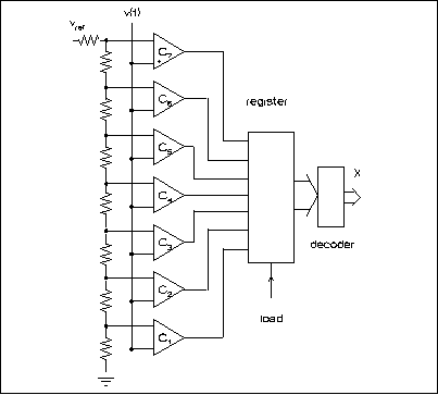 The situation is depicted for N = 3.
For comparator Cn, the logical true condition is set when v(t)>nvref/2N. It
is convenient to introduce the quantizing voltage v0=vref/2N. For a signal in
the interval nv0<v(t)#(n+1)v0 the set of outputs is of the
form ck=1, k=1,n and ck=0, k>n. The set of outputs can be considered as a 2N-1
bit word, Cn of weight n in which the n most significant bits are 1. The weights range from 0 to 2N-1
giving rise to 2N possible words. The load signal captures a specific word at time t, and a decoder
is used to produce an N-bit word X giving the binary integer code for the weight of C. The procedure is analogous
to the use of a ruler marked off in single units, say cm, to measure the length of a line. With the ruler aligned
at the starting point a one is assigned to each centimetre interval contained within the line and a zero for those
beyond the end of the line.
The situation is depicted for N = 3.
For comparator Cn, the logical true condition is set when v(t)>nvref/2N. It
is convenient to introduce the quantizing voltage v0=vref/2N. For a signal in
the interval nv0<v(t)#(n+1)v0 the set of outputs is of the
form ck=1, k=1,n and ck=0, k>n. The set of outputs can be considered as a 2N-1
bit word, Cn of weight n in which the n most significant bits are 1. The weights range from 0 to 2N-1
giving rise to 2N possible words. The load signal captures a specific word at time t, and a decoder
is used to produce an N-bit word X giving the binary integer code for the weight of C. The procedure is analogous
to the use of a ruler marked off in single units, say cm, to measure the length of a line. With the ruler aligned
at the starting point a one is assigned to each centimetre interval contained within the line and a zero for those
beyond the end of the line.
 Decoding by truth table or Karnaugh
map analysis to provide a combinational logic is rather unsuitable in this case. The word C to be decoded is extremely
long. The set of allowed words have very special structure and comprise a very small subset of the associated register
set RM where M = 2N-1. For example in the case shown with N = 3, the subset of legal
7-bit code words has 8 members out of the 128 members of the register set R7. However the special
structure may be used to advantage by defining the functions
Decoding by truth table or Karnaugh
map analysis to provide a combinational logic is rather unsuitable in this case. The word C to be decoded is extremely
long. The set of allowed words have very special structure and comprise a very small subset of the associated register
set RM where M = 2N-1. For example in the case shown with N = 3, the subset of legal
7-bit code words has 8 members out of the 128 members of the register set R7. However the special
structure may be used to advantage by defining the functions

over the set of comparator output words C. These functions have the property

and play a role for the subset that is accomplished by the min-terms for the entire register set. Each logical
variable yn(C) may be connected to a corresponding address line of a ROM, the contents of which contain
the appropriate X. For example in the case of N = 3, the variable y5(C) will be true for the comparator
word C5 = 1111100 and is connected to address line number 5. The contents of memory address 5 correspond
to the word X5=101, so that I10(X5) = 5.
In summary the ADC associates a digital output X with an analogue input v(t). The input-output relation is

that is, the N-bit word X which is the digital output is that word that represents n in the unsigned binary
integer code. The quantity n is the truncated integer value of the ratio of the input signal at time t to the quantization
voltage. Note that the integer value is defined so that integer(5.9999)=5 so that no rounding up is allowed. The
relation expressed by Eqn(3) is relevant to all ADCs. The input signal must lie within the range from 0 to vref
for proper operation. The digitization procedure corresponds to the many-to-one mapping of a segment of the real
number domain onto a single integer. For example, with the 3-bit converter shown and a 10 volt reference the interval
from 0 to 10 v is divided into 8 segments each of 1.25 v. The segment 6.25 < v(t)#
7.5v is mapped onto the integer 5. It is clearly advantageous to divide the interval into as many segments as possible
to minimize the uncertainty in the estimate of the input imposed by this mapping, referred to as the quantization
error. Thus if N were increased to 10, the width of a segment (v0 = vref/2N) would
decrease to 10/1024 v or just under 10 mV. The number of bits controls the ADC resolution, the device being said
to have N-bit resolution.
5.2 Counting Converter
 The result of a conversion using the
parallel converter is ready "in a flash", the conversion time being limited only by propagation delays.
It is difficult however to produce high resolution flash ADCs because of the large number of components required.
Thus to achieve 12-bit resolution it would be necessary to use 4095 comparators and a chain of 4096 precisely matched
resistors. Component number imposes a resolution limitation with this approach and alternative digitization methods
have been developed which circumvent this problem at the expense of conversion speed. A simple example is the counting
converter which employs a single comparator, an up-counter and a DAC in the arrangement shown. The measurement
process is initiated by a STRT pulse which zeros the counter and sets the flip flop. The counter then begins to
increment in response to the clock inducing a corresponding increment in the DAC output voltage. When the counter
has incremented so that the DAC output exceeds the input signal being measured the comparator resets the control
flip flop and the counter holds the number of clock pulses required. If this number of clock pulses is n = I10(X),
then the DAC is offset by the quantization voltage to output vDAC = (n+1)v0. This condition
is met when nv0 # v(t) < (n+1)v0.
The equality exists at the lower boundary of the segment in contrast to the flash ADC, but this difference is inconsequential
and the same input output relation described by Eqn(3) is appropriate. An important aspect of this type of conversion
is the conversion time. This can be written
The result of a conversion using the
parallel converter is ready "in a flash", the conversion time being limited only by propagation delays.
It is difficult however to produce high resolution flash ADCs because of the large number of components required.
Thus to achieve 12-bit resolution it would be necessary to use 4095 comparators and a chain of 4096 precisely matched
resistors. Component number imposes a resolution limitation with this approach and alternative digitization methods
have been developed which circumvent this problem at the expense of conversion speed. A simple example is the counting
converter which employs a single comparator, an up-counter and a DAC in the arrangement shown. The measurement
process is initiated by a STRT pulse which zeros the counter and sets the flip flop. The counter then begins to
increment in response to the clock inducing a corresponding increment in the DAC output voltage. When the counter
has incremented so that the DAC output exceeds the input signal being measured the comparator resets the control
flip flop and the counter holds the number of clock pulses required. If this number of clock pulses is n = I10(X),
then the DAC is offset by the quantization voltage to output vDAC = (n+1)v0. This condition
is met when nv0 # v(t) < (n+1)v0.
The equality exists at the lower boundary of the segment in contrast to the flash ADC, but this difference is inconsequential
and the same input output relation described by Eqn(3) is appropriate. An important aspect of this type of conversion
is the conversion time. This can be written

where f is the clock frequency and t is a constant reflecting propagation delays
etc. The first term is the most important and it should be noted that this contribution depends on n and hence
the magnitude of the signal. For high resolution ADCs the conversion time may become considerable. Thus for a 13-bit
ADC, if n=6000 and f=1Mhz, the conversion time would be somewhat greater than 6 milliseconds. One rather serious
aspect of this in the circuit shown is that there is considerable uncertainty in the time at which the measurement
is actually made, ie the t in v(t). Note that the time at which the conversion is complete can be sensed as the
positive going edge of the NOT BUSY signal.
5.3 Sample and Hold
 A common practice used when it is desired
to precisely define the time at which the signal measurement is made, is to employ a sample and hold circuit at
the ADC input. The signal is connected to a series type linear gate. With the sample high the linear gate output
follows the input so long as the charging time of the capacitor and input resistance is short on the time scale
of significant signal variations. If the sample is set low at time ts the signal value v(ts)
is stored on the capacitor. The operational amplifier merely isolates the capacitor because of its high input impedance.
The arrangement is referred to as a voltage follower since the op amp output must equal its input in this arrangement.
Thus in a typical measurement the sample variable is set low at the start of a measurement and held low during
the conversion. It may be returned to the high state at the end of conversion signified by the return of the NOT
BUSY level to high.
A common practice used when it is desired
to precisely define the time at which the signal measurement is made, is to employ a sample and hold circuit at
the ADC input. The signal is connected to a series type linear gate. With the sample high the linear gate output
follows the input so long as the charging time of the capacitor and input resistance is short on the time scale
of significant signal variations. If the sample is set low at time ts the signal value v(ts)
is stored on the capacitor. The operational amplifier merely isolates the capacitor because of its high input impedance.
The arrangement is referred to as a voltage follower since the op amp output must equal its input in this arrangement.
Thus in a typical measurement the sample variable is set low at the start of a measurement and held low during
the conversion. It may be returned to the high state at the end of conversion signified by the return of the NOT
BUSY level to high.
5.4 Tracking ADC
The tracking ADC is a modification of the counting converter particularly suited to signals which are relatively
stable. An up-down counter is used and is not reset after each measurement. The comparator output is not used to
control the clock input which is always present, but instead controls the counting mode. Thus if the comparator
output is high signifying the current DAC output is greater than the signal the count down mode is in effect. If
the signal is greater than the DAC output at any time then the corresponding low comparator output sets the counter
in the up mode. Thus the contents of the counter are continually updated and the ADC essentially follows or tracks
the signal. The ability of the ADC to follow variations in the input is governed by a quantity referred to as the
slew rate, a measure of the maximum output rate of change in general. After n clock pulses the DAC output increases
by nv0 volts. The time taken is n/fc, where fc is the clock frequency. The slew
rate is thus v0fc volts per second. Input variations which occur at rates less than this
amount will be tracked successfully. For input variations at a rate exceeding the slew rate it will not be possible
for the ADC to "keep up".
5.5 Successive Approximation ADC
While digitization with a parallel ADC is similar to measuring a length with a ruler, the action of a successive
approximation converter has analogies with the procedure of weighing a sample. Consider a balance designed for
a range of 16 g (equivalent to vref). The method underlying the counting converter corresponds to the
use of 15, 1g standards (v0). The unknown sample (v(t)) is placed on one pan of the balance (comparator)
and the minimum number of standards placed on the second pan required to exceed the weight of the unknown is then
determined. However this is not the efficient procedure. The set of standards used correspond to 8,4,2 and 1 g.
The standard procedure is to test the largest weight and either leave it on the balance if the sample is heavier
or remove it. The procedure is then repeated for each of the test weights in turn in descending order. Notice that
for any sample exactly 4 tests are made, while a variable number up to 15 are required in the methodology of the
counting converter. The successive approximation approach represents a procedure or algorithm to be implemented
using a digital system in which a measurement cycle involves a fixed set of N-steps for an N-bit converter. This
situation requires the use of a time state generator. The variable weight of the test weights may be accomplished
using a standard binary code arrangement, in which a test of weight 2N-n corresponds to setting bit
xn high.

In the arrangement shown, the 5-phase time state generator (N+2-phase in general) is driven by the clock so
that the positive going clock edge occurs at the middle of each phase. The three RS flip flops have both clocked
and direct resets. The latter are indicated by d where they are used in FF2 and FF3. Circuitry not shown issues
the start measure and hold sample commands. At T1 time FF1 set is high and the rest of the flip flops
are reset directly. When FF1 is clocked the DAC holds 100, giving an output of 4v0. If the input signal
is greater than or equal to 4v0, the comparator output is low. At T2 clock time the DAC input
is 110 and the output is 6v0. If on the other hand the signal is less than 4v0 the comparator
output is high and FF1 is reset at T2 so the DAC input is 010 and the output 2v0. At T3
time the process is repeated, with FF2 being reset or not depending on the comparator output and the action of
the least significant bit is tested. At T4 the result for the LSB is determined by the comparator output
and the decision made whether to retain this bit or not is made. T5 time indicates the end of the conversion
process. To again stress the analogy with weighing, if the DAC output is made higher (heavier) than the sample
by the addition of a bit, the comparator goes high, the bit is removed and testing moves on to the next bit of
lower significance. If adding a bit is insufficient to make the DAC output exceed the sample, that bit is retained,
ie the test weight is left on the pan.
5.6 Voltage-to-Time Converters
 These converters, typified by the Wilkinson
type are based upon generating a ramp voltage the basis of which is the integrating op-amp shown in the diagram.
If the input is constant the output varies linearly with time, within the limits of the dynamic range imposed by
the power supply. The input v(t') indicated in the diagram should not be confused with the signal to be measured.
These converters, typified by the Wilkinson
type are based upon generating a ramp voltage the basis of which is the integrating op-amp shown in the diagram.
If the input is constant the output varies linearly with time, within the limits of the dynamic range imposed by
the power supply. The input v(t') indicated in the diagram should not be confused with the signal to be measured.
In the situation of a constant input, v(t') = -vref the output can be written

If the integrator output is compared with a sampled signal voltage v, then the time required for the ramp to
increase to the sample is given by

The time interval is digitized by counting clock pulses during the period T, accomplished by enabling an up
counter for this interval. The contents of the counter at the end of the conversion is then
a word X coding for the integer n = I10(X) where

with the choice of circuit parameters so that

Eqn(7) becomes the standard ADC input-output relation. As can be seen from Eqn(6)the conversion time is variable,
depending on the size of the signal being measured, a feature in common with the counting converter. In essence
the Wilkinson converter essentially operates on the same principle as the counting converter with the DAC replaced
by the ramp voltage generator.
5.7 Dual-slope Converter
A modification of the Wilkinson converter is the dual slope converter shown below.

At the start of the measurement the N-bit counter and the carry flip flop, designated c are zeroed. Thus the
linear gate with the signal input is enabled. The integrator op-amp output is a negative going ramp which continues
as the counter increments since the comparator output remains high. At the 2N th clock pulse the counter
overflows setting the carry bit. The signal linear gate is disabled and the reference linear gate is enabled. The
op-amp output now rises linearly from the negative value to which it was driven by integration during connection
to the signal. When the op-amp output reaches zero the comparator level goes low, shutting off further clock inputs
to the counter and indicating the end of the conversion. Since the signal was integrated for 2N clock
pulses the voltage at the time -vref is applied is

The signal now rises at a rate of vref/RC so the time T required to reach 0 volts and switch the
comparator is given by

The contents of the counter at the end of the conversion code for the integer n where

again yielding the usual result. In this case however the result is completely independent of the values of
fc, R or C. This has the advantage of stability, since these parameters are susceptible to temperature
variations for example. The penalty to be paid is the increased conversion time which now becomes

5.8 Summary
The ADC is a device with two analogue inputs, the signal, or a held sample of the signal, v(t) and the reference
voltage vref, and a digital output consisting of the N-bit word X = {xi, i = 1,N}. The input
output relation is

where I10(X) is the decimal integer represented by X in the standard binary code for unsigned
integers. Extension to signed and fractional operation is possible. The quantity vref is often supplied
internally to the ADC and determines the operating range, 0<v(t)<vref. Ideally the effect is to
divide the range into equal intervals of magnitude vref/2N=v0, the quantizing
voltage, and assign the signal magnitude to one of the ordered intervals. Clearly the finer the interval the more
accurate will be the estimate of the signal. This leads to the attribute of resolution controlled by the number
of bits N. The goal of high resolution is countered by practical limitations. In the case of the flash ADC an enormous
number of identical components is required. In all other cases the price paid is increased conversion time, ie
a limitation on the operating speed of the device. With this regard, the successive approximation ADC is the most
efficient (excluding the flash ADC) in that the number of operations is fixed at N+2, while for the rest it varies
with 2N, say for a half scale input.
The flash and DAC-based ADCs are all essentially potentiometric devices relying on resistor chains to determine
the division of the range into intervals. Because the precision of resistors is limited in reality the intervals
or not identical, leading to non-linearity. This is expressed in two ways, integral non-linearity and differential
non-linearity. The first is based upon analysis of a graph of the input output relation which for high resolution
should be a straight line. A straight line is drawn through the end points of the actual curve and the relative
maximum departure is quoted. Differential linearity is a measure of the constancy of the intervals and is expressed
as the maximum relative deviation from the average. The voltage to time converters circumvent this problem and
are generally superior with regard to linearity. In this case departures from linear operation result from non-ideal
performance of the ramp generator.