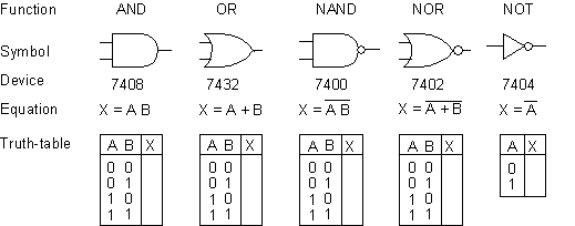
1. Complete the truth-tables for the following five basic logic elements and test the operation of at least one
of them.
2.
3.
4.
5. Design a half-adder circuit which forms the sum and carry of two bits.
6. Design a full-adder circuit which forms the sum and carry of three bits.
7. Design a digital circuit which will produce the sum of two 2-bit numbers.
8. Design a digital comparator which takes as input two 2-bit words A(a1, a0) and B(b1, b0). The outputs of the circuit are A>B, A=B and A<B.
9. Design a priority encoder for three possible inputs A, B, and C. The inputs are in order of descending priority such that A takes priority over B, and B over C. The output is a binary code indicating the presence of the input with the highest priority. Thus the output will be 3 for priority A, 2 for B, 1 for C and 0 for no input.
10. Design an interrupt priority encoder. The purpose of this circuit is to indicate when a device requests service and to identify by means of an identifying code or vector the requesting device possessing the highest priority. For this exercise there will be 8 inputs assigned codes 0 to 7. There will be four output lines. One output indicates that one or more devices are active, i.e., requesting service. The remaining three outputs are to provide the binary code of the device with the highest priority, where 0 is the highest and 7 is the lowest priority.
11. Design a circuit which takes a 4-bit input and produces the corresponding Hamming code. Display the 7-bit word on the lights with the format C1C2D1C3D2D3D4.